Organic compound and electronic device

A technology of organic compounds and electronic devices, applied in organic chemistry, chemical instruments and methods, circuits, etc., can solve the problems of performance degradation, luminous efficiency reduction, driving voltage increase of light-emitting devices, etc., to improve life characteristics, enhance injection and transmission. , the effect of inhibiting material crystallization

Active Publication Date: 2020-04-21
SHAANXI LIGHTE OPTOELECTRONICS MATERIAL CO LTD
View PDF1 Cites 22 Cited by
  • Summary
  • Abstract
  • Description
  • Claims
  • Application Information

AI Technical Summary

Problems solved by technology

[0003] Generally, when an organic electroluminescent device is driven at high temperature, there are problems such as an increase in driving voltage, a decrease in luminous efficiency, and a shortened lifespan, resulting in a decrease in the performance of the organic electroluminescent device

Method used


Image

  • Organic compound and electronic device
  • Organic compound and electronic device
  • Organic compound and electronic device

Examples


preparation example Construction

[0063] The preparation method of the compound of the embodiment of the present invention is described in detail below:

[0064] Synthesis of compound 1

[0065]

[0066] Magnesium strips (15.44g, 643.5mmol) and diethyl ether (100mL) were placed in a dry round bottom flask under nitrogen, and iodine (119mg) was added. Then a solution of ether (200mL) dissolved with 2-bromobiphenyl 2-bromotoluene (50.00g, 214.49mmol) was slowly dropped into the flask, and after the addition was completed, the temperature was raised to 35°C and stirred for 3 hours; the reaction solution was lowered to 0°C, a solution of ether (200mL) dissolved with adamantanone (48.33g, 321.7mmol) was slowly dropped into it, and after the addition was completed, the temperature was raised to 35°C and stirred for 6 hours; the reaction solution was cooled to room temperature, and added 5% hydrochloric acid to pH<7, stirred for 1 hour, added diethyl ether (200mL) for extraction, combined the organic phases, drie...

Embodiment 1

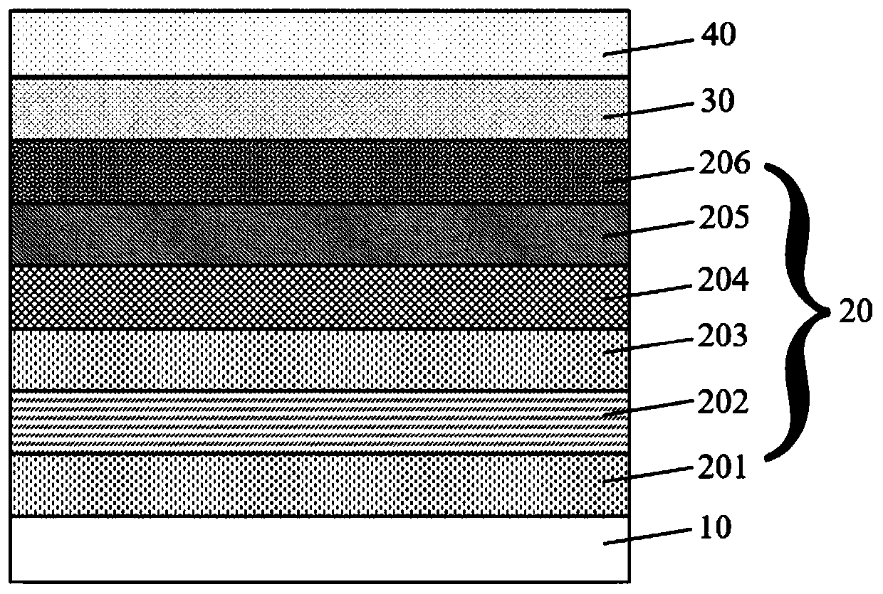
[0183] The anode 10 is prepared by the following process: the thickness is The ITO substrate was cut into a size of 40mm × 40mm × 0.7mm, and it was prepared into a top emission experimental substrate with a cathode overlapping area, an anode and an insulating layer pattern by using a photolithography process, using ultraviolet ozone and O 2 :N 2 Plasma is used for surface treatment to increase the work function of the anode (experimental substrate) and to clean the experimental substrate.

[0184] On the experimental substrate (anode 10) vacuum evaporation HAT-CN to form a thickness of The hole injection layer (HIL) 201.

[0185] NPB is vacuum evaporated on the hole injection layer 201 to form a thickness of The hole transport layer (HTL) 202.

[0186] Evaporate TCTA on the hole transport layer 202 to form a thickness of Electron blocking layer (EBL) 203 .

[0187] α, β-ADN is used as the main body, and BD-1 is doped at a doping ratio of 3%, and evaporated on the ele...

Embodiment 2-19

[0197] The organic electroluminescence device was fabricated by the same method as in Example 1, except that, when forming the electron transport layer (ETL) 206, the compounds shown in Table 1 were used instead of Compound 1.


PUM

PropertyMeasurementUnit
Electron mobilityaaaaaaaaaa

Abstract

The invention provides an organic compound and an electronic device containing the organic compound, and belongs to the technical field of organic materials. The structure of the organic compound is shown as the following formula (1), wherein the structure of Y is shown as the following formula (2) or (3). The organic compound is used in an electronic device such as an organic electroluminescent device, and can improve lifetime characteristics, efficiency characteristics, electrochemical stability, and thermal stability of the organic electroluminescent device and reduce a driving voltage.

Description

technical field [0001] The present invention relates to the technical field of organic materials, in particular, to an organic compound and an electronic device containing the organic compound. Background technique [0002] In recent years, organic electroluminescent device (OLED: Organic electroluminescent device), as a new generation of display technology, has gradually entered people's field of vision. A common organic electroluminescent device is composed of an anode, a cathode, and more than one organic layer arranged between the cathode and the anode. When a voltage is applied to the cathode and anode, the two electrodes generate an electric field. Under the action of the electric field, the electrons on the cathode side move to the light-emitting layer in the organic layer, and the electrons on the anode side also move to the light-emitting layer. The two combine to form excitons in the light-emitting layer. The exciton releases energy in the excited state, and emits...

Claims


Application Information

Patent Timeline
IPC IPC(8): C07D251/24C07D405/10C07D409/10C07D403/10C07D401/10C07D213/22C07D401/14C09K11/06H01L51/42H01L51/50H01L51/46H01L51/54
CPCC07D251/24C07D405/10C07D409/10C07D403/10C07D401/10C07D213/22C07D401/14C09K11/06C09K2211/1011C09K2211/1014C09K2211/1029C09K2211/1044C09K2211/1059C09K2211/1088C09K2211/1092H10K85/615H10K85/624H10K85/631H10K85/626H10K85/654H10K85/6572H10K85/6574H10K85/6576H10K30/50H10K50/16Y02E10/549C09K2211/1018
Inventor 马天天张孔燕曹佳梅
Owner SHAANXI LIGHTE OPTOELECTRONICS MATERIAL CO LTD
Why Eureka
Try Eureka