Nitrogen-containing compound, and electronic component and electronic device using same

A nitrogen compound, chemical bond technology, applied in electrical components, electrical solid devices, circuits, etc., can solve problems such as low electron mobility, reduced device luminous efficiency, and unfavorable energy conservation.

Active Publication Date: 2020-10-30
SHAANXI LIGHTE OPTOELECTRONICS MATERIAL CO LTD
View PDF13 Cites 5 Cited by
  • Summary
  • Abstract
  • Description
  • Claims
  • Application Information

AI Technical Summary

Problems solved by technology

[0003] Generally speaking, electron transport materials are compounds with electron-deficient nitrogen-containing heterocyclic groups. Most of them have high electron affinity, so they have a strong ability to accept electrons. However, compared with hole transport materials, The electron mobility of common electron transport materials, such as octahydroxyquinoline aluminum, is much lower than the hole mobility of hole transport materials, so in OLED devices, on the one hand, it will lead to the imbalance of carrier injection and transport. The recombination probability of holes and electrons is reduced, thereby reducing the luminous efficiency of the device. On the other hand, electron transport materials with lower electron mobility will lead to an increase in the operating voltage of the device, thereby affecting power efficiency and detrimental to energy saving.

Method used


Image

  • Nitrogen-containing compound, and electronic component and electronic device using same
  • Nitrogen-containing compound, and electronic component and electronic device using same
  • Nitrogen-containing compound, and electronic component and electronic device using same

Examples


Embodiment 1

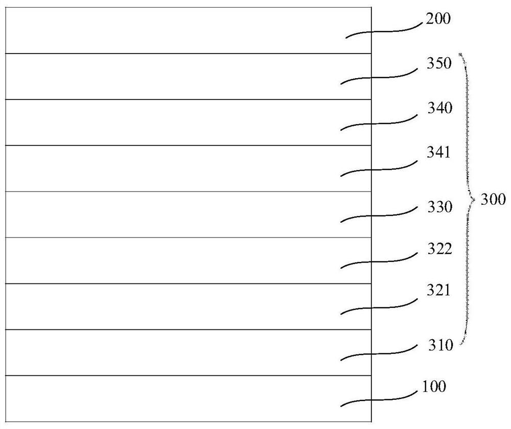
[0247] Embodiment 1 blue organic electroluminescent device

[0248] The anode was prepared by the following process: the thickness was The ITO substrate (manufactured by Corning) was cut into a size of 40mm×40mm×0.7mm, and it was prepared into an experimental substrate with cathode, anode and insulating layer patterns by photolithography process, using ultraviolet ozone and O 2 :N 2 Plasma surface treatment was performed to increase the work function of the anode (experimental substrate) and to remove scum.

[0249] F4-TCNQ was vacuum evaporated on the experimental substrate (anode) to form a thickness of The hole injection layer (HIL), and HT-01 is evaporated on the hole injection layer to form a thickness of hole transport layer.

[0250] EB-01 was vacuum evaporated on the hole transport layer to form a thickness of electron blocking layer.

[0251] On the electron blocking layer, BH-01 and BD-01 are co-evaporated at a ratio of 98%: 2%, forming a thickness of org...

Embodiment 2~30

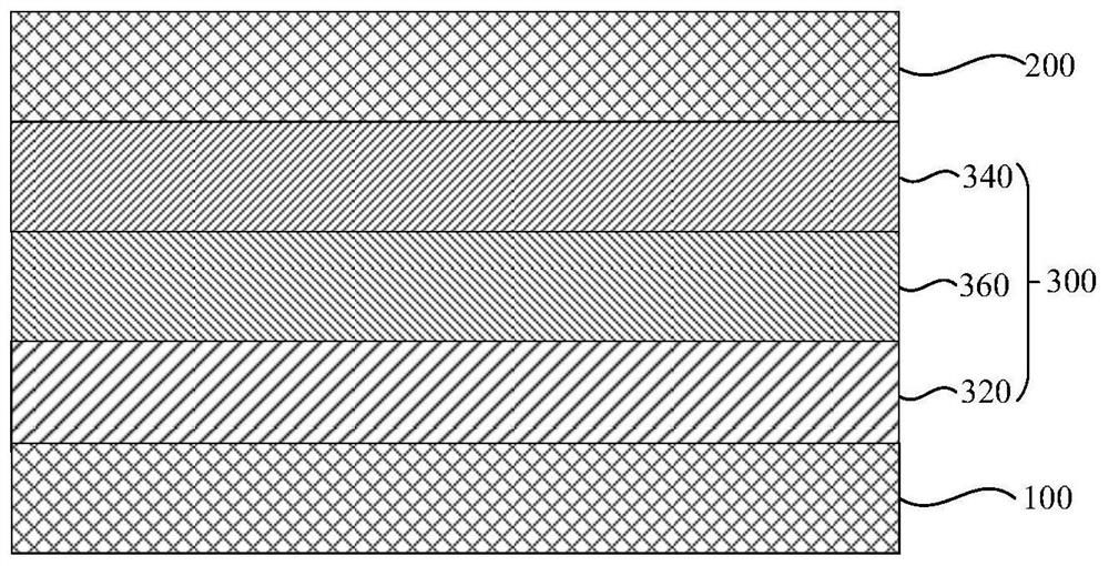
[0257] The organic electroluminescence device was prepared by the same method as in Example 1, except that the nitrogen-containing compound A-1 was replaced with the nitrogen-containing compounds shown in Table 9 when preparing the electron transport layer.

Embodiment 31

[0259] The organic electroluminescence device is prepared by the same method as in Example 1, the difference is only that, when forming the hole blocking layer, the nitrogen-containing compound B-11 of the present application is used instead of the compound ET-01, and when forming the electron transport layer , the nitrogen-containing compound A-1 of the present application was replaced by compound ET-01.


PUM


Abstract

The invention relates to a nitrogen-containing compound having a structural formula as described in the specification. In the formula, a ring A and a ring B are each independently selected from benzene rings or fused aromatic rings having 10-14 ring-forming carbon atoms, and at least one of the ring A and the ring B is selected from the fused aromatic rings having 10-14 ring-forming carbon atoms;L is selected from single-bond, substituted or unsubstituted arylene groups having 6-30 carbon atoms and substituted or unsubstituted heteroarylene groups having 3-30 carbon atoms; and Het is a substituted or unsubstituted nitrogen-containing heteroaryl group with a carbon atom number of 3 to 60. The nitrogen-containing compound provided by the invention can improve the luminous efficiency of an organic electroluminescent device and improve the conversion efficiency of a photoelectric conversion device using the nitrogen-containing compound.

Description

technical field [0001] The application belongs to the technical field of organic materials, and specifically provides a nitrogen-containing compound and electronic components and electronic devices using the same. Background technique [0002] An organic light-emitting element is a representative example of an organic electronic element. In general, the organic light emitting phenomenon refers to a phenomenon in which electrical energy is converted into light energy by using an organic substance. An organic light emitting element utilizing an organic light emitting phenomenon generally has a structure including an anode and a cathode and an organic layer therebetween. Among them, in order to improve the efficiency and stability of the organic light-emitting element, the organic layer is often formed by a multilayer structure composed of different substances, for example, a hole injection layer, a hole transport layer, a light-emitting layer, an electron transport layer, an ...

Claims


Application Information

Patent Timeline
IPC IPC(8): C07D213/57C07D215/06C07D235/18C07D237/08C07D239/26C07D239/74C07D241/42C07D251/24C07D401/04C07D401/10C07D401/14C07D403/04C07D403/10C07D405/04C07D405/10C07D405/14C07D409/04C07D409/10C07D409/14C07D413/10C07D417/10C07D491/048C07D495/04H01L51/54H01L51/50
CPCC07D251/24C07D401/10C07D405/04C07D409/04C07D401/04C07D405/10C07D403/10C07D403/04C07D413/10C07D417/10C07D239/74C07D237/08C07D241/42C07D235/18C07D215/06C07D495/04C07D491/048C07D409/10C07D405/14C07D409/14C07D401/14C07D239/26C07D213/57H10K85/624H10K85/626H10K85/654H10K85/657H10K85/6576H10K85/6572H10K85/6574H10K50/16H10K50/18Y02E10/549C07D215/12C07D407/14C07D407/04H10K85/652C07B2200/05
Inventor 杨敏南朋
Owner SHAANXI LIGHTE OPTOELECTRONICS MATERIAL CO LTD
Why Eureka
Try Eureka