Compounds, photoelectric conversion devices and electronic devices

A photoelectric conversion and compound technology, applied in the field of organic materials, can solve the problems of performance degradation of light-emitting devices, increase in operating voltage, decrease in luminous efficiency, etc., and achieve the effect of improving the molecular weight of materials, low driving voltage, and enhancing injection and transmission.

Active Publication Date: 2020-08-11
SHAANXI LIGHTE OPTOELECTRONICS MATERIAL CO LTD
View PDF1 Cites 0 Cited by
  • Summary
  • Abstract
  • Description
  • Claims
  • Application Information

AI Technical Summary

Problems solved by technology

[0003] At present, when organic electroluminescent devices are driven at high temperatures, there will be problems such as increased operating voltage, reduced luminous efficiency, and shortened lifespan, resulting in a decline in the performance of organic electroluminescent devices.

Method used


Image

  • Compounds, photoelectric conversion devices and electronic devices
  • Compounds, photoelectric conversion devices and electronic devices
  • Compounds, photoelectric conversion devices and electronic devices

Examples


Embodiment 1

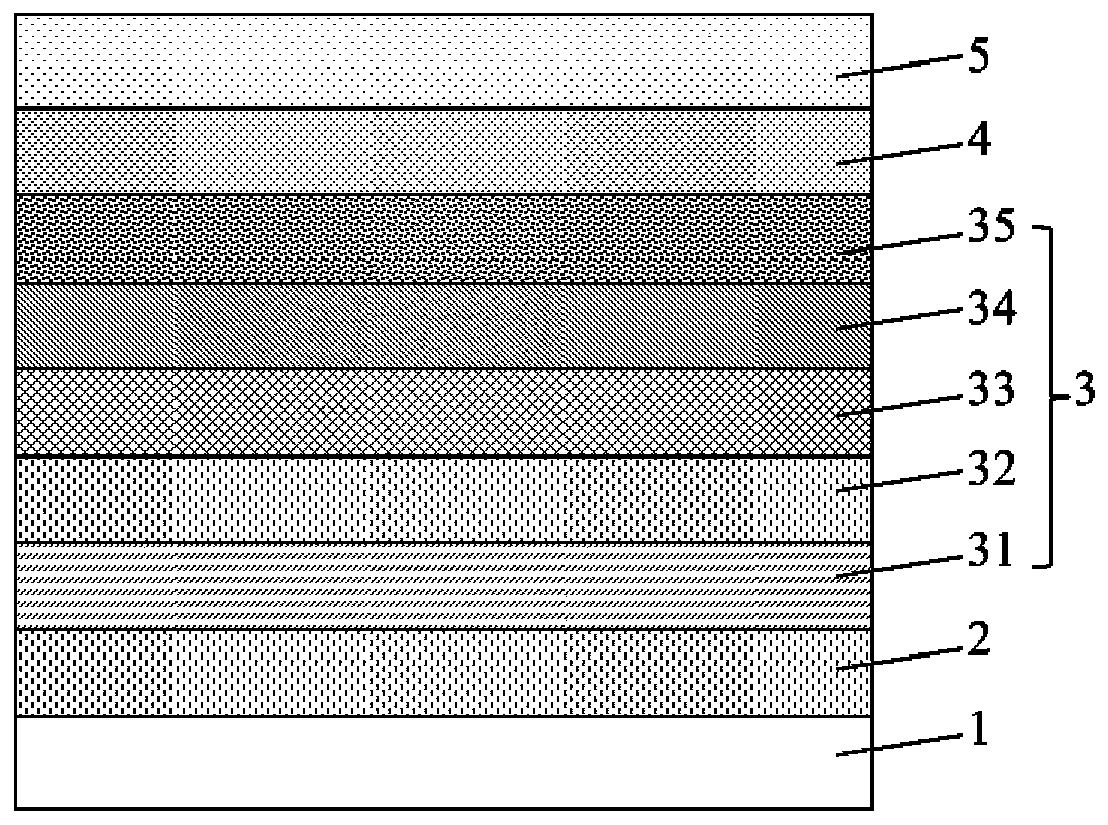
[0201] Anode 1 was prepared by the following process: the thickness of ITO was The ITO substrate (manufactured by Corning) was cut into a size of 40mm (length) × 40mm (width) × 0.7mm (thickness), and it was prepared into a pattern with a cathode 5 overlapping area, an anode 1 and an insulating layer by using a photolithography process. Top emission experimental substrate, using ultraviolet ozone and O 2 :N 2 Plasma was used for surface treatment to increase the work function of the anode 1 (experimental substrate) and to clean the experimental substrate.

[0202] Vacuum-deposit m-MTDATA (4,4',4"-tris(N-3-methylphenyl-N-phenylamino)triphenylamine) on the experimental substrate (anode 1) to form a thickness of The hole injection layer 2 (HIL), and on the hole injection layer 2 vacuum evaporated NPB (N,N'-diphenyl-N,N'-(1-naphthyl)-1,1'-bi benzene-4,4'-diamine) to form a thickness of The hole transport layer 31 (HTL).

[0203] Evaporate TCTA (4,4',4 "-tris(carbazol-9-yl) ...

Embodiment 2~17

[0208] An organic electroluminescent device was fabricated by the same method as in Example 1 except that the compounds shown in Table 1 were each used in forming the electron transport layer 35 (ETL).


PUM

PropertyMeasurementUnit
electron mobilityaaaaaaaaaa

Abstract

The disclosure provides a compound represented by formula I, a photoelectric conversion device and an electronic device, belonging to the technical field of organic materials. The compound can reduce the operating voltage of the photoelectric conversion device, improve the luminous efficiency of the photoelectric conversion device, and prolong the life of the device.

Description

technical field [0001] The present disclosure relates to the technical field of organic materials, in particular, to a compound, a photoelectric conversion device and an electronic device. Background technique [0002] In recent years, with the development of semiconductor technology, photoelectric conversion devices have been widely used. For example, organic electroluminescent devices (OLED, Organic electroluminescent device) have gradually entered people's field of vision as a new generation of display devices. A common organic electroluminescent device is composed of an anode, a cathode and an organic layer arranged between the cathode and the anode. When a voltage is applied to the cathode and anode, the two electrodes generate an electric field. Under the action of the electric field, the electrons on the cathode side and the holes on the anode side move to the light-emitting layer at the same time, and they combine to form excitons in the light-emitting layer, and the...

Claims


Application Information

Patent Timeline
Patent Type & Authority Patents(China)
IPC IPC(8): C07D213/16C07D239/26C07D251/24C07D401/04C07D401/10C07D401/14H01L51/54H01L51/50H01L51/46
CPCC07D251/24C07D239/26C07D401/14C07D213/16C07D401/04C07D401/10H10K85/624H10K85/626H10K85/615H10K85/654H10K50/16Y02E10/549C07D213/06H10K50/171H10K30/451
Inventor 马天天杨敏南朋
Owner SHAANXI LIGHTE OPTOELECTRONICS MATERIAL CO LTD
Why Eureka
Try Eureka