Array substrate and display device

An array substrate and display area technology, applied in static indicators, nonlinear optics, instruments, etc., can solve the problems of low aperture ratio, poor display picture, high power consumption, etc., to increase aperture ratio, avoid defects, and reduce power consumption. consumption effect

Pending Publication Date: 2020-05-08
BOE TECH GRP CO LTD +1
View PDF11 Cites 8 Cited by
  • Summary
  • Abstract
  • Description
  • Claims
  • Application Information

AI Technical Summary

Problems solved by technology

[0005] Embodiments of the present invention provide an array substrate and a device to solve the problems of high power consumption, low aperture ratio and poor display screen in existing dual-gate drive display devices

Method used


Image

  • Array substrate and display device
  • Array substrate and display device
  • Array substrate and display device

Examples


Embodiment Construction

[0026] In order to make the purpose, technical solution and advantages of the present invention clearer, the array substrate and the display device provided by the embodiments of the present invention will be further described in detail below in conjunction with the accompanying drawings. Obviously, the described embodiments are only part of the embodiments of the present invention. , but not all examples. Based on the embodiments of the present invention, all other embodiments obtained by persons of ordinary skill in the art without making creative efforts belong to the protection scope of the present invention.

[0027] The shapes and sizes of the components in the drawings do not reflect the real scale of the array substrate, but are only intended to schematically illustrate the content of the present invention.

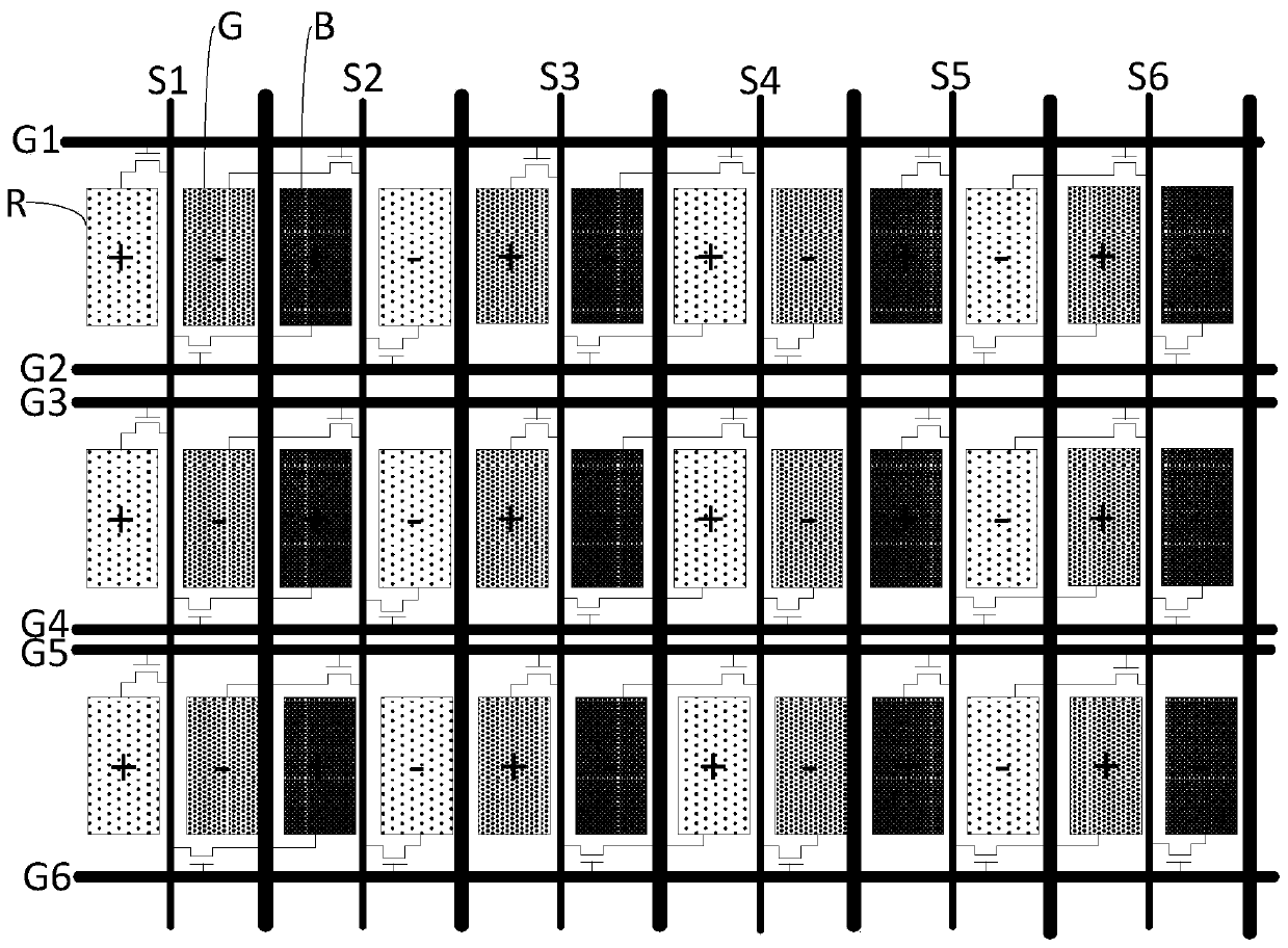
[0028] The inventors of the present application found that, in the related art dual-gate drive liquid crystal display device, the pixels turned on during the high...


PUM


Abstract

The invention discloses an array substrate and a display device. At least two columns of data lines correspondingly and electrically connected with sub-pixels with the same polarity are electrically connected with the same bonding pad located in a non-display area; in this way, the bridging positions of different columns of sub-pixels are arranged in the non-display area, on one hand, the apertureopening ratio of the pixels can be increased, the display brightness can be improved, and on the other hand, the problem that in the display area in the prior art, due to bridging of data lines and the pixels, pixels are coupled, and consequently a display image is poor can be avoided; besides, when the array substrate provided by the invention displays a pure-color picture, the same data line can output constant output voltage, so that the power consumption when the pure-color picture is displayed is effectively reduced.

Description

technical field [0001] The present invention relates to the field of display technology, in particular to an array substrate and a display device. Background technique [0002] Liquid Crystal Display (LCD) devices are widely used in modern information equipment, such as monitors, televisions, mobile phones and digital products, due to their advantages of light weight, low power consumption, low radiation and easy portability. The main structure of the liquid crystal display device is composed of an array substrate, a color filter substrate and a liquid crystal layer filled between the two substrates. [0003] With the development of high-resolution display, not only the power consumption of the display device is gradually increasing, but also the cost of the driving IC is continuously increasing. In order to reduce the cost of the driver IC, related technologies have proposed an array substrate driven by dual gates. The dual gate driver can not only reduce the number of dat...

Claims


Application Information

Patent Timeline
Patent Type & Authority Applications(China)
IPC IPC(8): G02F1/1362G02F1/1345G09G3/36
CPCG02F1/136286G02F1/13452G09G3/3614
Inventor 孟昭晖孙伟韩文超李路康丛林
Owner BOE TECH GRP CO LTD
Why Eureka
Try Eureka