Composite light conversion layer substrate for Micro-LED array device and preparation method of composite light conversion layer substrate

A technology of composite light and conversion layer, applied in semiconductor devices, optical filters, electrical components, etc., can solve problems such as poor film quality

Active Publication Date: 2020-05-08
CHANGCHUN INST OF OPTICS FINE MECHANICS & PHYSICS CHINESE ACAD OF SCI
View PDF5 Cites 6 Cited by
  • Summary
  • Abstract
  • Description
  • Claims
  • Application Information

AI Technical Summary

Problems solved by technology

[0005] In order to solve the problem of poor film-forming quality on the surface of existing quantum dot materials applied to Micro-LEDs or light conversion substrates, the present invention provides a composite light conversion layer substrate for Micro-LED array devices and a preparation method thereof. It can solve the "coffee ring effect" in the formation of the quantum dot film layer, and the effect is remarkable

Method used


Image

  • Composite light conversion layer substrate for Micro-LED array device and preparation method of composite light conversion layer substrate
  • Composite light conversion layer substrate for Micro-LED array device and preparation method of composite light conversion layer substrate
  • Composite light conversion layer substrate for Micro-LED array device and preparation method of composite light conversion layer substrate

Examples


Embodiment Construction

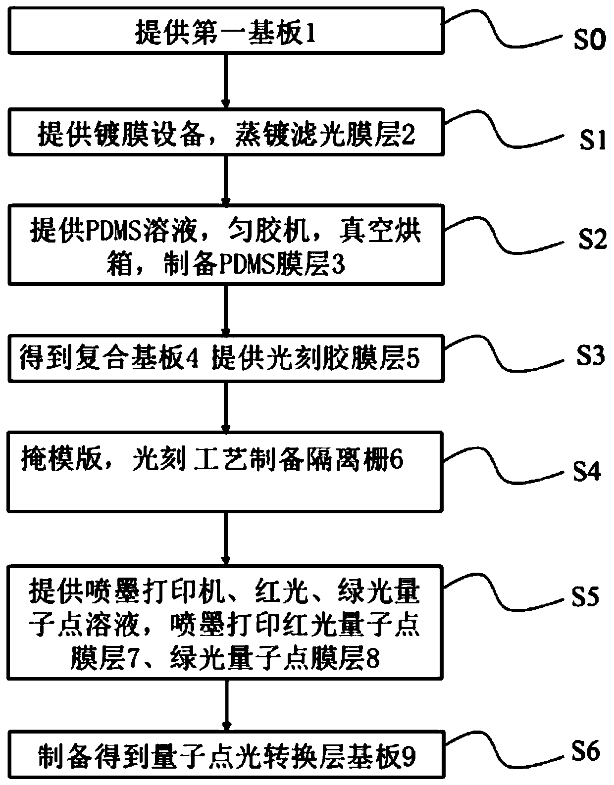
[0035] The idea, specific structure and technical effects of the present invention will be clearly and completely described below in conjunction with the embodiments and accompanying drawings, so as to fully understand the purpose, features and effects of the present invention. Apparently, the described embodiments are only some of the embodiments of the present invention, rather than all of them. Based on the embodiments of the present invention, other embodiments obtained by those skilled in the art without creative efforts belong to The protection scope of the present invention.

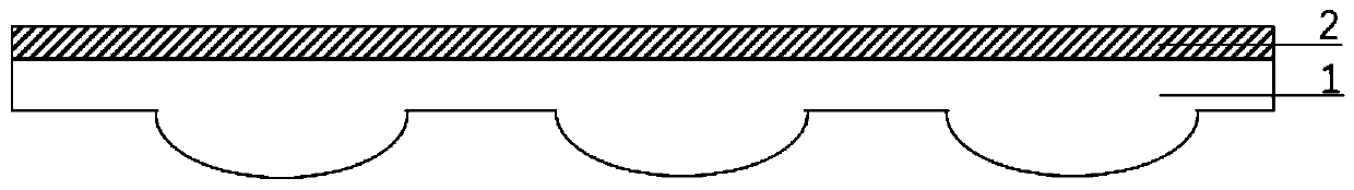
[0036] Such as Figure 8 As shown, a composite light conversion layer substrate for Micro-LED array devices, the substrate includes a first substrate 1, a filter film layer 2 set on the first substrate 1, a filter film layer 2 set on the PDMS film layer 3, several photoresist isolation barriers 6 arranged on the PDMS film layer 3, red light quantum dot film layer 7 and green light quantum dot fil...


PUM

PropertyMeasurementUnit
thicknessaaaaaaaaaa
thicknessaaaaaaaaaa
thicknessaaaaaaaaaa

Abstract

The invention provides a composite light conversion layer substrate for a Micro-LED array device and a preparation method of the composite light conversion layer substrate, and relates to the technical field of Micro-LED display. The substrate comprises a first substrate body, a filter film layer arranged on the first substrate body, a PDMS film layer arranged on the filter film layer, photoresistisolation gates arranged on the PDMS film layer, red light quantum dot film layers and green light quantum dot film layers, wherein the red light quantum dot film layers and the green light quantum dot film layers are arranged in grooves between the photoresist isolation gates respectively. According to the composite substrate, blue light emission of the Micro-LED blue light excitation light source can be effectively filtered out; meanwhile, due to the introduction of the flexible PDMS film layer in the composite substrate, the coffee ring effect occurring after ink-jet printing of a low-concentration quantum dot solution is effectively solved, the substrate is inverted above the blue light Micro-LED array, and full-color display based on the blue light Micro-LED array is achieved.

Description

technical field [0001] The invention relates to the field of Micro-LED display technology, in particular to a composite light conversion layer substrate for a Micro-LED array device and a preparation method thereof. Background technique [0002] Micro-LED is the latest achievement of further miniaturization of traditional LED with the continuous development of micro-nano processing technology in recent years. The size of the light-emitting unit of traditional LED is usually larger than 100 μm, while the size of a single Micro-LED is less than 100 μm. The Micro-LED display device is a two-dimensional array display device composed of high-density pixel light-emitting units integrated on a single chip. [0003] At present, there are many researches on the manufacturing process of monochrome Micro-LED display devices, and the manufacturing process is relatively mature. There are currently three main ways to prepare full-color Micro-LED display devices: three-color LED chip asse...

Claims


Application Information

Patent Timeline
Patent Type & Authority Applications(China)
IPC IPC(8): H01L33/50G02B5/20
CPCG02B5/20H01L33/505H01L2933/0041
Inventor 梁静秋王家先陶金王维彪吕金光秦余欣李阳赵永周
Owner CHANGCHUN INST OF OPTICS FINE MECHANICS & PHYSICS CHINESE ACAD OF SCI
Why Eureka
Try Eureka