Display device
A technology of display equipment and light-emitting components, which is applied in the directions of optics, instruments, electrical components, etc., and can solve problems such as insufficient brightness and inability to optimally design reflective liquid crystal displays.
- Summary
- Abstract
- Description
- Claims
- Application Information
AI Technical Summary
Problems solved by technology
Method used
Image

Examples
no. 1 approach 〕
[0021] In the following, "same layer" means formed with the same material in the same process, "lower layer" means formed in the previous process compared with the layer of the comparison object, and "upper layer" means the same layer as the comparison object The layer is compared to the meaning formed in the subsequent process. In addition, "overlapping" means that two members have an overlapping portion in a plan view, and also includes the case where other members are interposed or not interposed between these two members.
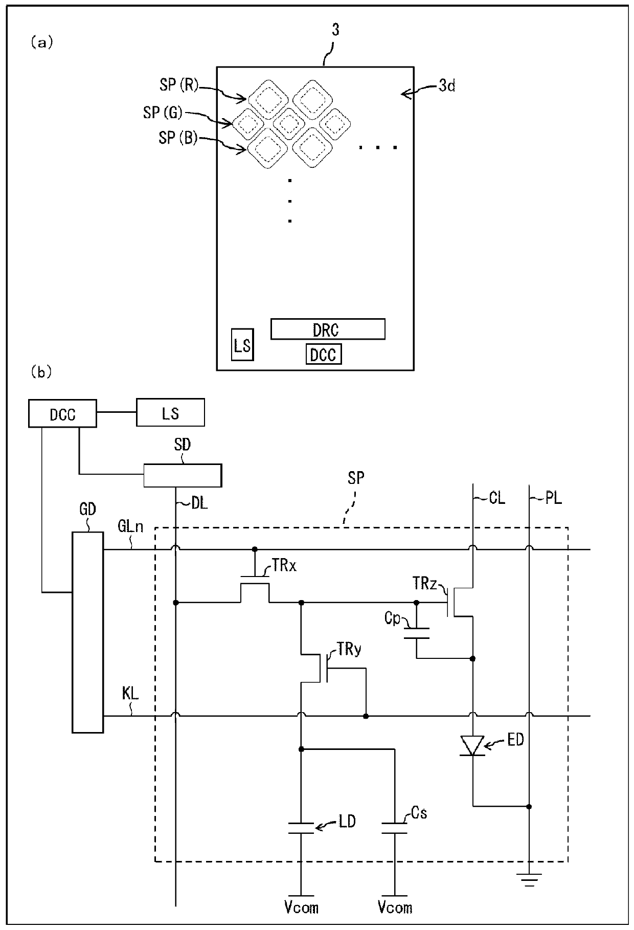
[0022] figure 1 (a) is a plan view showing the display device of the first embodiment, figure 1 (b) is a circuit diagram showing a configuration example of a sub-pixel. like figure 1 As shown in (a), the display device 3 of the first embodiment includes a display portion 3d including a red sub-pixel SP(R), a green sub-pixel SP(G), and a blue sub-pixel SP(B). ; a drive circuit DRC, which drives the display portion 3d; an external light sensor LS; and...
no. 2 approach 〕
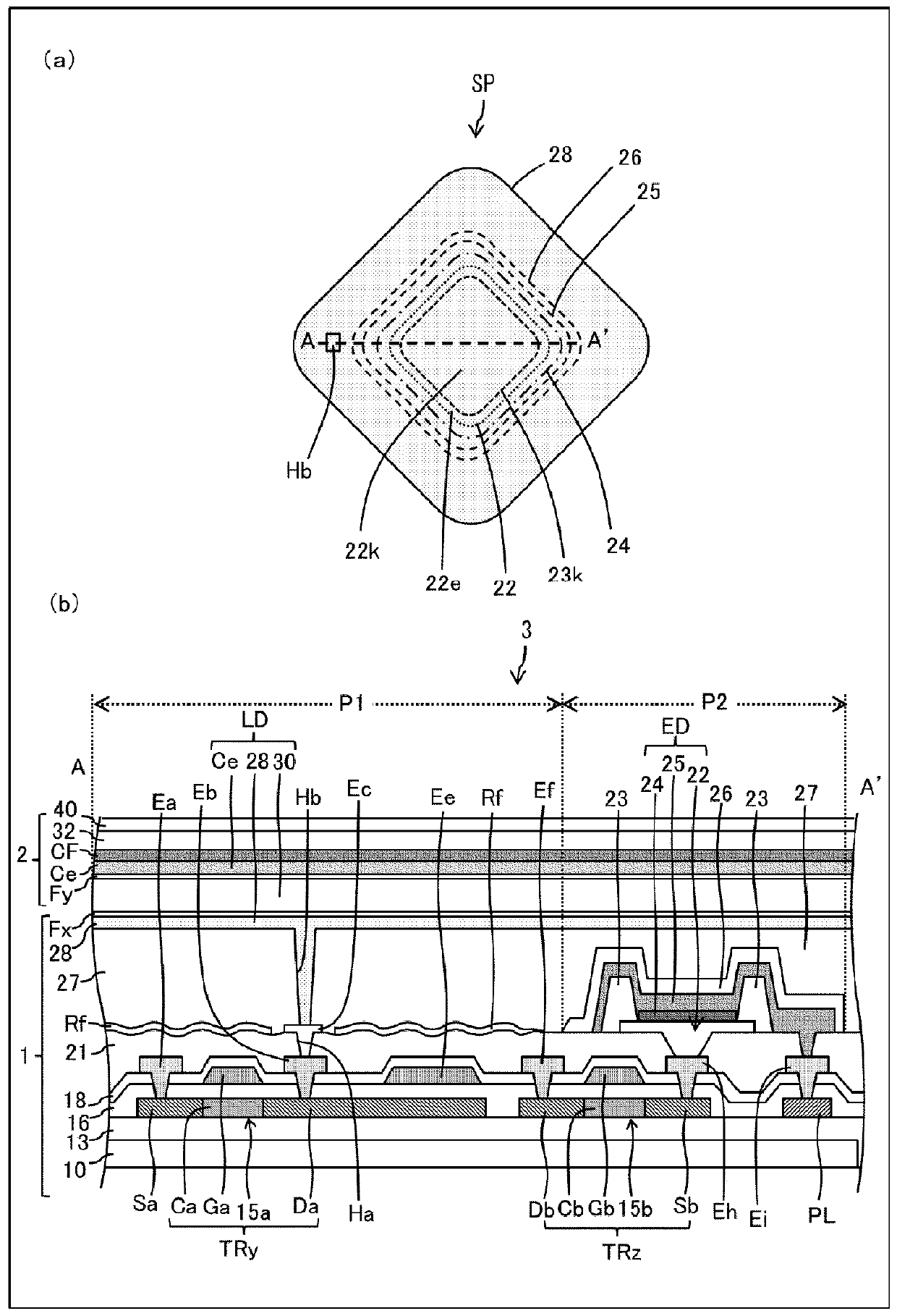
[0057] Figure 5 is a cross-sectional view showing the display device of the second embodiment. In the second embodiment, the buffer film Bf is provided in the same layer as the electrode cover film 23 covering the anode 22 of the light-emitting element. The buffer film Bf includes a region with an uneven surface, and the light reflection film Rf is formed on this region. The pixel electrode 28 is formed on the light reflection film Rf. The pixel electrode 28 (first portion) is connected to the transistor TRy through the contact hole Ha of the interlayer insulating film 21 and the contact hole Hc of the buffer film Bf.
[0058] In this manner, by forming the light reflection film Rf on the buffer film Bf formed in the same process as the electrode cover film 23, the number of manufacturing steps can be reduced. In this case, by aligning the upper surface level of the buffer film Bf with the upper surface level of the packaging film 26, the thickness (gap) of the liquid cryst...
no. 3 approach 〕
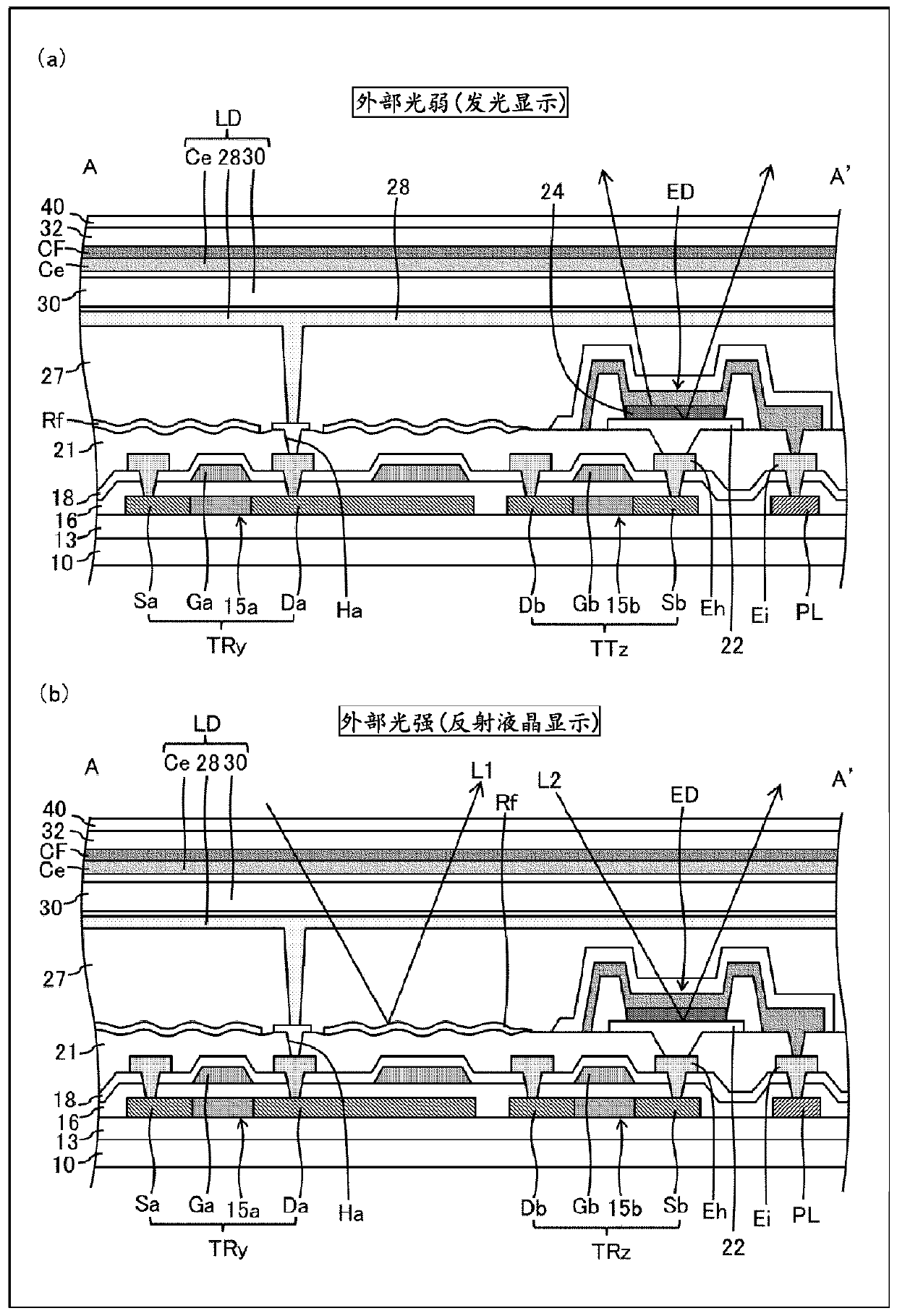
[0060] Image 6 is a cross-sectional view showing the display device of the second embodiment. In the second embodiment, the light-reflecting film Rf having an uneven surface is superimposed on the light-emitting element ED, and the surface of the anode 22 in the same layer (formed in the same process) as the light-reflecting film Rf is also formed with unevenness. In this way, reflected light can be effectively diffused even in the region where the light emitting element ED is formed, and the quality of reflective liquid crystal display can be improved. In addition, since the edge of the packaging film 26 is in contact with the inorganic film, that is, the light reflection film Rf, the adhesion between the two is good, and the sealing effect is good. Image 6 Here, since the light reflection film Rf and the cathode 25 are in contact with each other, the cathode potential can be supplied to the light reflection film Rf. A configuration in which the light reflection film Rf i...
PUM
| Property | Measurement | Unit |
|---|---|---|
| Thickness | aaaaa | aaaaa |
Abstract
Description
Claims
Application Information
 - R&D Engineer
- R&D Manager
- IP Professional
- Industry Leading Data Capabilities
- Powerful AI technology
- Patent DNA Extraction
Browse by: Latest US Patents, China's latest patents, Technical Efficacy Thesaurus, Application Domain, Technology Topic.
© 2024 PatSnap. All rights reserved.Legal|Privacy policy|Modern Slavery Act Transparency Statement|Sitemap