
Semiconductor substrate thinning method

A semiconductor and substrate technology, applied in the field of semiconductor substrate thinning, can solve problems such as cumbersome operation and poor flatness of semiconductor substrates, and achieve the effects of simplifying the thinning process, reducing the cost of thinning, and ensuring flatness

Pending Publication Date: 2020-05-19
YANGTZE MEMORY TECH CO LTD
View PDF10 Cites 0 Cited by
  • Summary
  • Abstract
  • Description
  • Claims
  • Application Information

AI Technical Summary

Problems solved by technology

[0006] The invention provides a method for thinning a semiconductor substrate, which is used to solve the problems that the existing semiconductor substrate thinning method is cumbersome to operate and the flatness of the thinned semiconductor substrate is poor, so as to improve the performance of semiconductor devices

Method used


Image

  • Semiconductor substrate thinning method
  • Semiconductor substrate thinning method
  • Semiconductor substrate thinning method

Examples


Embodiment Construction

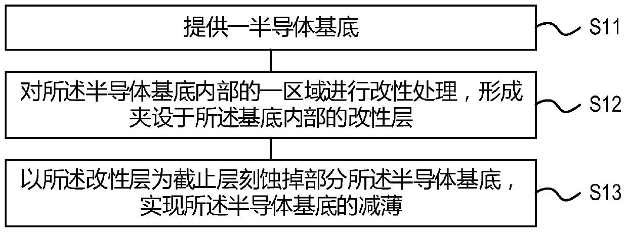
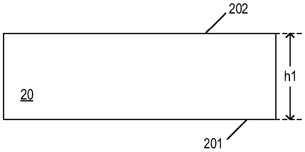
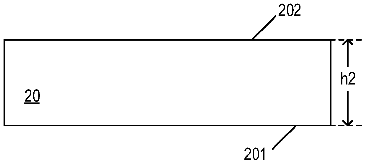
[0029] The specific implementation of the semiconductor substrate thinning method provided by the present invention will be described in detail below in conjunction with the accompanying drawings.

[0030] Currently, in the process of thinning the semiconductor substrate of a semiconductor device, it is mainly accomplished through multi-step chemical mechanical polishing steps, or a combination of multi-step chemical mechanical polishing and wet etching processes. However, the chemical mechanical polishing process itself is complex, time-consuming, and expensive; in addition, the chemical mechanical polishing process still has great challenges in controlling the flatness of the polished semiconductor substrate surface.

[0031] Therefore, in order to optimize the thinning process of the semiconductor substrate, reduce the semiconductor manufacturing cost and improve the semiconductor production efficiency, this specific embodiment provides a method for thinning the semiconducto...


PUM

PropertyMeasurementUnit
thicknessaaaaaaaaaa

Abstract

The invention relates to the technical field of semiconductor manufacturing, in particular to a semiconductor substrate thinning method. The semiconductor substrate thinning method comprises the following steps: providing a semiconductor substrate; carrying out modification processing on an area in the semiconductor substrate to form a modified layer clamped in the semiconductor substrate; and etching off a part of the semiconductor substrate by taking the modified layer as a cut-off layer to realize thinning of the semiconductor substrate. According to the invention, the thinning process of the semiconductor substrate is simplified, and the thinning cost is reduced; and the flatness of the thinned surface can be ensured, and the performance of the semiconductor device is improved.

Description

technical field [0001] The invention relates to the technical field of semiconductor manufacturing, in particular to a method for thinning a semiconductor substrate. Background technique [0002] With the development of planar flash memory, the production process of semiconductors has made great progress. However, in recent years, the development of planar flash memory has encountered various challenges: physical limits, existing development technology limits, and storage electron density limits. In this context, in order to solve the difficulties encountered in planar flash memory and pursue lower production costs per unit storage unit, various three-dimensional (3D) flash memory structures have emerged, such as 3D NOR (3D or not) flash memory and 3D NAND (3D NAND) flash memory. [0003] Among them, 3D NAND memory takes its small size and large capacity as the starting point, and the design concept of highly integrated storage units stacked in three-dimensional mode is to...

Claims


Application Information

Patent Timeline
Patent Type & Authority Applications(China)
IPC IPC(8): H01L21/322H01L21/265H01L21/306
CPCH01L21/322H01L21/26506H01L21/306
Inventor 朱宏斌
Owner YANGTZE MEMORY TECH CO LTD
Features
  • Generate Ideas
  • Intellectual Property
  • Life Sciences
  • Materials
  • Tech Scout
  • Unparalleled Data Quality
  • Higher Quality Content
  • 60% Fewer Hallucinations
Learn More