Wide-voltage-range input type non-isolated double-switch wide-gain boost direct-current converter
A technology of DC converter and double switch, which is applied in the direction of converting DC power input to DC power output, adjusting electrical variables, and output power conversion devices, and can solve problems such as narrow boosting range and weak boosting capacity
- Summary
- Abstract
- Description
- Claims
- Application Information
AI Technical Summary
Problems solved by technology
Method used
Image

Examples
Embodiment 1
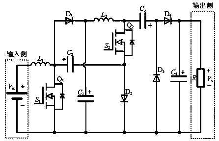
[0019] 1) Topology
[0020] Such as figure 1 Shown is the topology of the proposed converter of the present invention. The input side of the converter is used V in Indicates a DC generating unit with a low voltage level, with a resistive load on the output side R Indicates the load on the DC bus side, used for the DC bus voltage V o express. The input side and the output side are connected by the proposed dual-switch wide-gain DC boost unit, which consists of two inductors L 1 , L 2 , four capacitors C 1 ~ C 4 , 6 power devices Q 1 , Q 2 、D 1 ~D 4 pose, Q 1 and Q 2 The drive signal is used respectively S 1 and S 2 express.
[0021] 2) Wide voltage gain
[0022] The converter proposed in this patent contains two power switches and requires two drive signals S 1 , S 2 , in theory S 1 S 2 There are four combinations, namely "11, 10, 00, 01" ("1" means the switch is on, and "0" means the switch is off). However, since the proposed converter uses t...
Embodiment 2
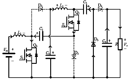
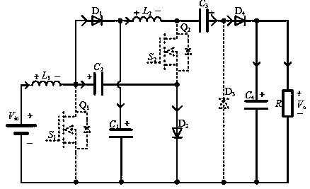
[0048] Below to figure 1 The novel wide-gain quasi-Z source switched capacitor boost DC converter topology shown, figure 2 , 3 The topological equivalent circuit diagram of and Figure 4 The important working waveforms when the new topology is running stably, and the principle of the solution in the first embodiment will be described. In one carrier cycle, the converter experiences two switching states. The two switch states are described below respectively.
[0049] (1) S 1 S 2 =11, the equivalent circuit of this state is as figure 2 shown. according to Figure 4 The topological working waveform, in this working mode, the power switch tube Q 1 , Q 2 conduction, the diode D 1 、D 2 、D 4 off, D 3 conduction. V in by Q 1 To inductance L 1 charge; capacitor C 1 and C 2 by Q 1 , Q 2 Series to inductor L 2 charge; capacitor C 2 by Q 1 , Q 2 and D 3 Give C 3 charge; capacitor C 4 give load R powered by.
[0050] (2) S 1 S 2 =00, the equiv...
PUM
 Abstract
Description
Claims
Application Information
 - R&D
- Intellectual Property
- Life Sciences
- Materials
- Tech Scout
- Unparalleled Data Quality
- Higher Quality Content
- 60% Fewer Hallucinations
Browse by: Latest US Patents, China's latest patents, Technical Efficacy Thesaurus, Application Domain, Technology Topic, Popular Technical Reports.
© 2025 PatSnap. All rights reserved.Legal|Privacy policy|Modern Slavery Act Transparency Statement|Sitemap|About US| Contact US: help@patsnap.com