Method for testing warping degree of wafer

A test method and wafer technology, applied in semiconductor/solid-state device test/measurement, electrical components, circuits, etc., can solve problems such as insufficient accuracy, reduce the influence of gravity, and the test method is convenient and simple, reducing deformation effect

Active Publication Date: 2020-05-22
JIAXING BAISHENG PHOTOELECTRIC
View PDF7 Cites 6 Cited by
  • Summary
  • Abstract
  • Description
  • Claims
  • Application Information

AI Technical Summary

Problems solved by technology

[0004] The object of the present invention is to provide a method for testing wafer warpage, which can effectively solve the problem of gravity by testing the wafer in a vertical state. The problem that affects the test and leads to insufficient accuracy

Method used


Image

  • Method for testing warping degree of wafer
  • Method for testing warping degree of wafer
  • Method for testing warping degree of wafer

Examples


Embodiment Construction

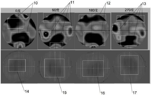
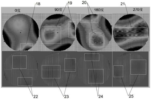
[0025] Embodiments of the invention are described in detail below, examples of which are illustrated in the accompanying drawings. The embodiments described below by referring to the figures are exemplary and are intended to explain the present invention and should not be construed as limiting the present invention.

[0026] In describing the present invention, it should be understood that the terms "center", "longitudinal", "transverse", "length", "width", "thickness", "upper", "lower", "front", " The orientation or positional relationship indicated by "rear", "left", "right", "vertical", "horizontal", "top", "bottom", "inner" and "outer" are based on the orientation or position shown in the drawings The positional relationship is only for the convenience of describing the present invention and simplifying the description, but does not indicate or imply that the referred device or element must have a specific orientation, be constructed and operated in a specific orientation,...


PUM


Abstract

The invention discloses a method for testing the warping degree of a wafer, and the method comprises the following steps: (1) vertically arranging a standard flat mirror, and enabling the standard flat mirror to be parallel to the direction of gravity; (2) loading a wafer; (3) adjusting the distance between the wafer and the standard flat mirror; (4) adjusting the wafer to be parallel to the standard flat mirror in a face-to-face manner; (5) starting a test module, enabling the test module to perform parallel movement scanning relative to the standard flat mirror, and respectively sampling thedistance from a probe of the sensor to the wafer and the distance from the probe of the sensor to the standard flat mirror through the sensor arranged on the test module; (6) performing data processing program processing on the obtained distance sampling value to obtain a warping degree parameter of the wafer. The method has the advantages that when the wafer is vertically placed for testing, therigidity in the wafer surface is high, the influence of gravity can be greatly reduced, deformation is reduced, and the testing method is convenient and simple.

Description

technical field [0001] The invention relates to the field of wafer surface parameter measurement, in particular to a method for testing wafer warpage. Background technique [0002] In integrated circuit on-chip manufacturing, in order to increase production capacity and reduce costs, large-size silicon wafers are used more and more widely; at the same time, in order to improve chip performance and packaging density, the development of three-dimensional packaging technology requires thinning of large-size silicon wafers . The residual stress generated during the thinning process causes the silicon wafer to warp and deform, which will increase the fragmentation rate of the silicon wafer during transportation and subsequent processing. The warping deformation of silicon wafer is an important technical index to evaluate the processing quality of silicon wafer, and it is also an important basis for analyzing the residual stress of silicon wafer processing and optimizing the thin...

Claims


Application Information

Patent Timeline
Patent Type & Authority Applications(China)
IPC IPC(8): H01L21/66
CPCH01L22/12H01L22/20
Inventor 陈跃华彭从峰卜志超陈时兴
Owner JIAXING BAISHENG PHOTOELECTRIC
Why Eureka
Try Eureka