Monitoring system and monitoring method for semiconductor manufacturing device

A technology for manufacturing devices and monitoring systems, which is applied in semiconductor/solid-state device manufacturing, measuring devices, and gas analyzer structure details, etc. It can solve the problems that the process cannot be monitored in real time, the product is defective, and the burden on operators is increased. Achieve the effect of avoiding bad products, reducing production costs and avoiding bad products

Pending Publication Date: 2020-05-26
CHANGXIN MEMORY TECH INC
View PDF4 Cites 3 Cited by
  • Summary
  • Abstract
  • Description
  • Claims
  • Application Information

AI Technical Summary

Problems solved by technology

[0004] However, since the existing technology cannot monitor the process in the reaction chamber of the semiconductor manufacturing device in real time, it is impossible to immediately find the defects such as air leakage, source deterioration, pollution, exhaust, etc., resulting in a la

Method used


Image

  • Monitoring system and monitoring method for semiconductor manufacturing device
  • Monitoring system and monitoring method for semiconductor manufacturing device
  • Monitoring system and monitoring method for semiconductor manufacturing device

Examples


Embodiment Construction

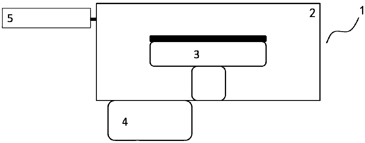
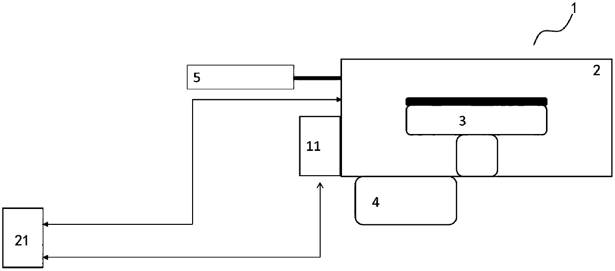
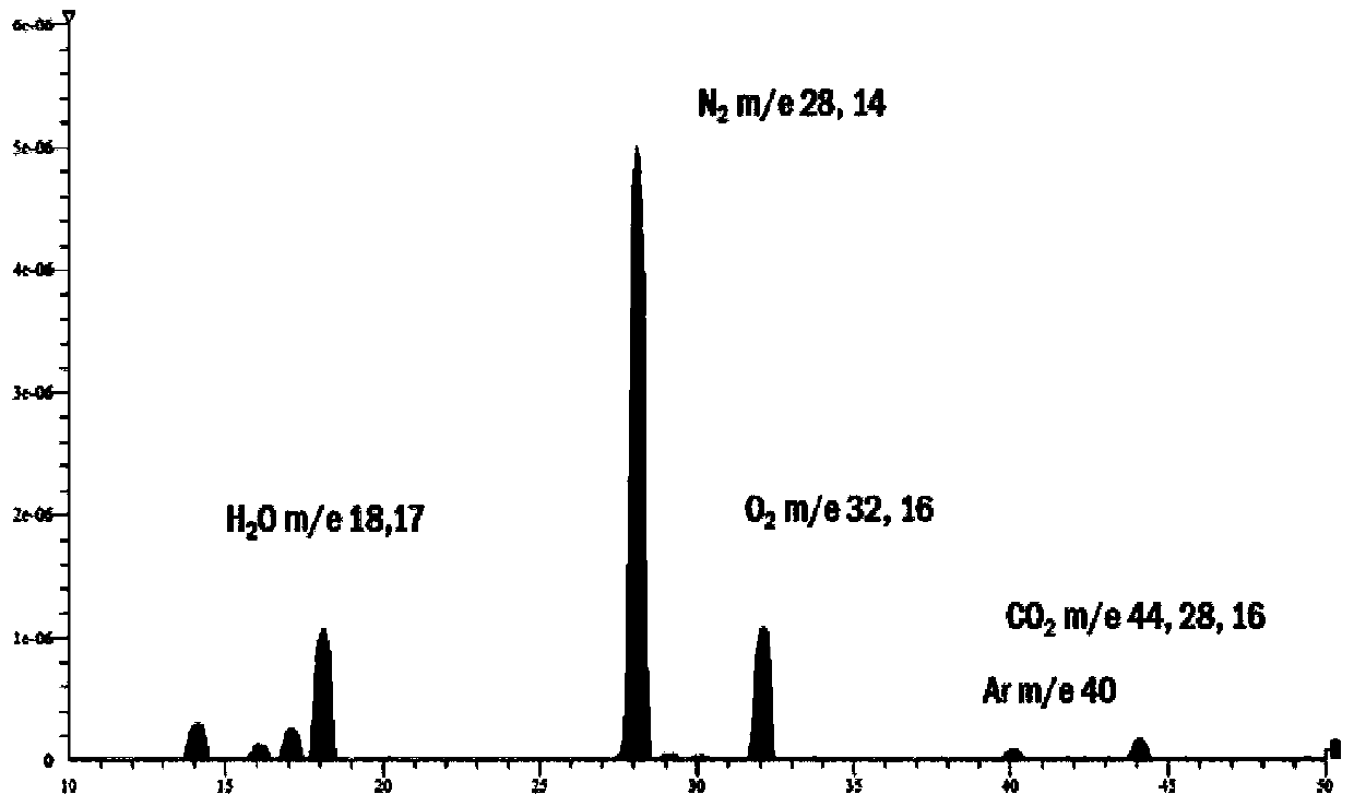
[0034] Embodiments of the present invention will be described in more detail below with reference to the accompanying drawings. Obviously, the embodiments of the present invention can be implemented through various embodiments, so the present invention should not be construed as being limited to the embodiments described below; in addition, the description of the following embodiments can make the present invention more comprehensive and complete, and enable those skilled in the art to more fully and clearly understand the concept of the embodiments of the present invention. The described features, structures, or characteristics can be combined in any combination in one or more embodiments. In the following description, numerous specific details are provided in order to give a thorough understanding of the embodiments of the present disclosure. However, those skilled in the art will appreciate that the technical solutions of the present disclosure may be practiced without one...


PUM


Abstract

The invention provides a monitoring system and a monitoring method for a semiconductor manufacturing device. The monitoring system comprises a semiconductor manufacturing device and a residual gas analyzer, wherein the semiconductor manufacturing device is provided with a reaction chamber for depositing a semiconductor; and the residual gas analyzer is arranged in the reaction chamber and is provided with a detection unit for detecting the state information in the reaction chamber in real time to obtain the real-time state information. The preparation process in the reaction chamber can be monitored in real time, so that the defects of air leakage, source deterioration, pollution, exhaust and the like can be found in time, a large number of bad products are prevented from being produced, and the production cost is greatly reduced. In addition, as manual monitoring is not needed in the preparation process, not only is the product defect caused by misoperation of operators avoided, but also the burden of the operators is greatly reduced.

Description

technical field [0001] The present invention relates to a semiconductor manufacturing device, in particular to a monitoring system and a monitoring method for the semiconductor manufacturing device. Background technique [0002] Currently, as semiconductors are widely used in digital products such as computers and mobile phones, the manufacturing process of semiconductor products has also received extensive attention. [0003] In an existing semiconductor manufacturing process, a chemical vapor deposition (Chemical Vapor Deposition: CVD) process, a physical vapor deposition (Physical Vapor Deposition: PVD) process, metal physical vapor deposition (metal Physical Vapor Deposition) and the like can be used to manufacture semiconductors. However, with the continuous deepening of device miniaturization, the size of semiconductor structures is getting smaller and smaller, especially when the critical dimensions of semiconductor products are reduced to below 30nm, the requirements...

Claims


Application Information

Patent Timeline
IPC IPC(8): H01L21/67G01N33/00
CPCH01L21/67253G01N33/0009
Inventor 不公告发明人
Owner CHANGXIN MEMORY TECH INC
Why Eureka
Try Eureka