Display device and manufacturing method thereof

A technology of a display device and a manufacturing method, applied in the field of display screens, can solve problems such as affecting production efficiency

Active Publication Date: 2020-05-26
XIAMEN SANAN OPTOELECTRONICS TECH CO LTD
View PDF8 Cites 2 Cited by
  • Summary
  • Abstract
  • Description
  • Claims
  • Application Information

AI Technical Summary

Problems solved by technology

However, mixing chips during the sorting proc

Method used


Image

  • Display device and manufacturing method thereof
  • Display device and manufacturing method thereof
  • Display device and manufacturing method thereof

Examples


Embodiment 1

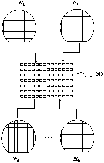
[0036] figure 2 A schematic diagram of a method for manufacturing an LED display screen implemented according to the present invention is shown. and figure 1The manufacturing method shown is completely different: after cutting the LED wafer into chips, step (2) is omitted in this method, that is, the LED chips are no longer rearranged, but the LED chips are assembled from W1~WN Chips are selected from among the wafers, and then placed directly on the circuit board 200 for installation. During the installation process, LED chips from different wafers can be mixed and arranged at the same time. The manufacturing method will be described in detail below in conjunction with the accompanying drawings.

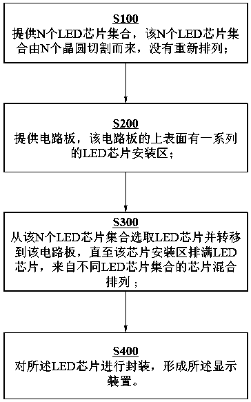
[0037] image 3 It is a flow chart of a manufacturing method of a light emitting diode display screen implemented according to the present invention. Such as image 3 As shown, the manufacturing method includes:

[0038] S100: Provide N LED chip sets, where the N LED chip set...

Embodiment 2

[0082] This embodiment provides an LED display screen, the LED display screen includes a display unit, the display unit includes a circuit board and a plurality of LED chips welded on the circuit board, the plurality of LED chips 100 are from different wafers, Chips from different wafers are mixed and arranged. The display unit is micro-modularized and includes a series of display sub-regions 100C, and the multiple display sub-regions constitute a required arrangement pattern. Each sub-region 100C can be an area such as M×N or M×K, wherein N is the number of LED chip sets, M and K are integers greater than 0, and the number of LED chips M×N or M×K is preferably 200 Below, preferably less than 100, such as 18, 24, 27, 36, 48, 54, or 72, or 81, etc., each sub-region 100C has the same LED chips and Arrangement order, the arrangement pattern of this sub-area can be selected according to the display requirements Figure 9~11 One of. Preferably, the display sub-areas are arranged...

Embodiment 3

[0087] This embodiment provides an LED display screen. Different from Embodiment 2, the LED chips in each display sub-area come from the same wafer, and each sub-area is randomly arranged, so that the chips in the screen are arranged in random numbers, and there is no Streaks or blocks of color difference / brightness and darkness, when modules and modules or screens are further assembled, there will be no streaks or block color differences / brightness and darkness.

[0088] Preferably, the number of LED chips in each sub-region is 1-25, preferably 4-16.

[0089] As a modification, the sub-regions can also be periodically arranged in the manner of horizontal reentry, vertical reentry, clockwise, counterclockwise, etc. Each period includes N sub-regions, and the LED chips in the N sub-regions are from N Each sub-region is preferably a region such as B×C, wherein B is an integer greater than 1, preferably 9-16, wherein the value of B:C is preferably 0.5-2. Preferably, there are so...


PUM


Abstract

The invention discloses a manufacturing method of a display device. The method comprises the following steps: providing N LED chip sets, wherein the N LED chip sets are formed by cutting N wafers andare not rearranged, the first LED chip set is produced from the first wafer, the second LED chip set is produced from the second wafer,..., the Nth LED chip set is produced from the Nth wafer, and N is an integer greater than 2; providing a circuit board (200), wherein the upper surface of the circuit board (200) is provided with a series of LED chip mounting areas (210); selecting LEDs from the NLED chip sets and transferring to the circuit board (200) until the chip mounting area (210) is full of the LED chips, and arranging the chips from different LED chip sets in a mixed mode; and packaging the LED chip to form the display device. The invention further provides a display device.

Description

technical field [0001] The invention relates to the technical field of display screens, in particular to an LED display device and a manufacturing method thereof. Background technique [0002] Light-emitting diodes have the characteristics of small size, long service life, colorful colors, and low energy consumption. They are widely used in lighting, displays, signal lights, backlights, toys and other fields. The LED display includes a plurality of LED chips arrayed on a printed circuit board. [0003] The existing manufacturing methods of LED display devices usually include the following steps: (1) LED chip manufacturers manufacture LED epitaxial wafers into LED chips; Rearrange on the same blue film 120; (3) Then the packaging manufacturer or the display manufacturer grabs the LED chip from the rearranged blue film and installs it on the circuit board 200, such as figure 1 shown. Further, in order to reduce brightness differences and / or color differences in different ar...

Claims


Application Information

Patent Timeline
IPC IPC(8): H01L21/67H01L27/15G09F9/33
CPCH01L21/67144H01L27/156G09F9/33
Inventor 林素慧彭康伟黄苡叡张中英何安和黄禹杰王锋
Owner XIAMEN SANAN OPTOELECTRONICS TECH CO LTD
Why Eureka
Try Eureka