Electronic detonator communication circuit and electronic detonator

A technology of electronic detonators and communication circuits, which is applied in fuzes, weapon accessories, offensive equipment, etc., can solve problems such as damage to electronic detonator communication conversion circuits, interference chip work, damage to electronic detonator chips, etc., to improve anti-interference ability and expand applications Scenes, effects released in time

Active Publication Date: 2020-06-05
杭州晋旗电子科技有限公司
View PDF10 Cites 4 Cited by
  • Summary
  • Abstract
  • Description
  • Claims
  • Application Information

AI Technical Summary

Problems solved by technology

The reverse superposition effect of differential mode interference will have a great impact on communication signals, especially in the process of delayed network detonation, the detonator detonated in the early stage will generate a strong differential mode interference signal, which is transmitted through the network bus When the electronic detonator is detonated in the later stage, a high superimposed voltage will be generated, and even the front-end communication conversion circuit of the electronic detonator will be damaged, which will be directly transmitted to the pins of the electronic detonator chip. The instantaneous high voltage will seriously interfere with the operation of the chip, causing the electronic detonator chip to Abnormal work or reset, in severe cases, may break down and damage the electronic detonator chip, directly causing the electronic detonator to fail or be scrapped, and bring unnecessary losses to the blasting operation

Method used


Image

  • Electronic detonator communication circuit and electronic detonator
  • Electronic detonator communication circuit and electronic detonator

Examples


Embodiment 1

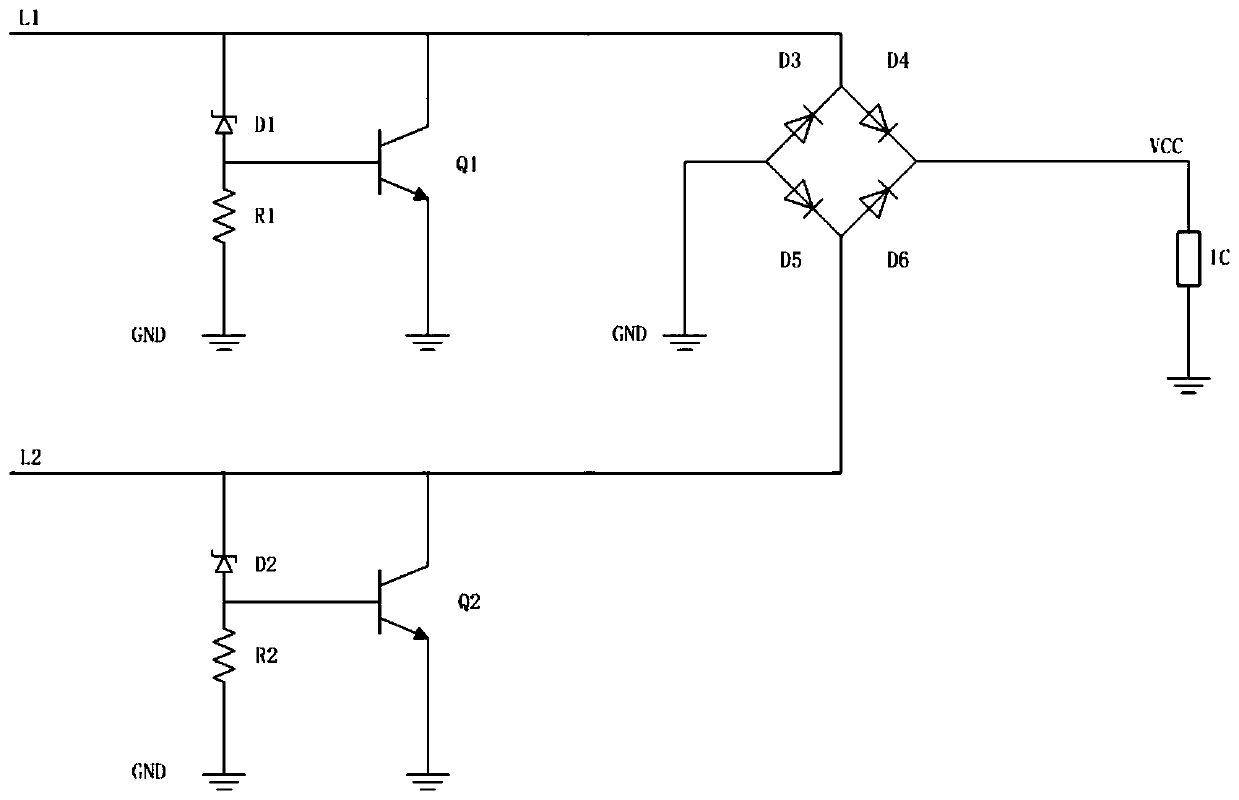
[0026] Such as figure 1 As shown, the present embodiment provides an electronic detonator communication circuit, including a communication bus L1, a communication bus L2, a rectifier circuit and a chip IC. The communication bus L2 is connected to the input end of the rectifier circuit respectively, that is, the communication bus L1 is connected between the cathode of D3 and the anode of D4, the communication bus L2 is connected between the cathode of D5 and the anode of D6, and the chip IC is connected to the output end of the rectification circuit , That is, between the cathode of D4 and the cathode of D6, and the other output terminal of the rectifier circuit, that is, between the anode of D3 and the anode of D5 is grounded. The electronic detonator detonator communicates with the electronic detonator through the communication bus L1 and the communication bus L2, and provides working power at the same time; since the electronic detonator uses a bipolar communication method, ...

Embodiment 2

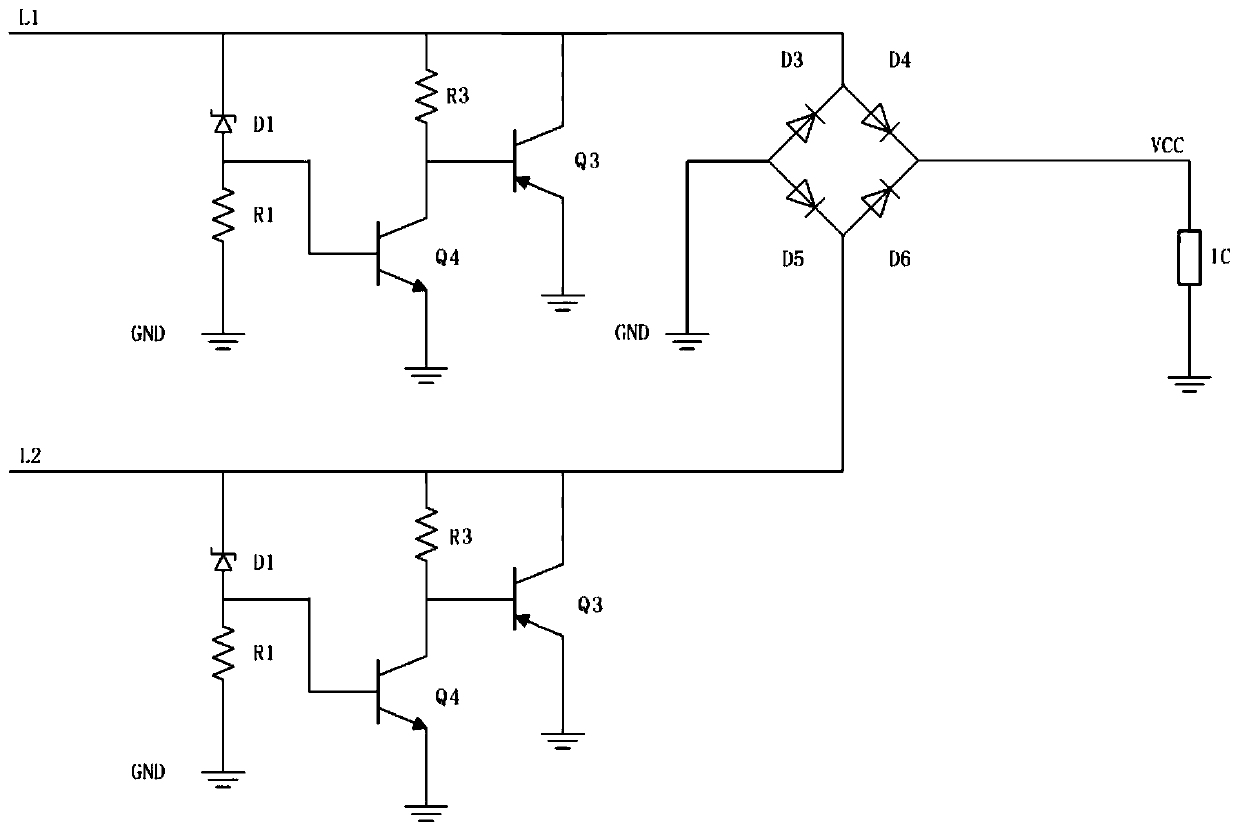
[0033] Such as figure 2 As shown, this embodiment provides an electronic detonator communication circuit. The difference from Embodiment 1 is that in this embodiment, the switching element is a PNP transistor Q3, and the differential mode suppression circuit also includes a conversion element, which is an NPN transistor Q4, which is used to protect the voltage when differential mode interference occurs. The high level of the component transient voltage suppression diode D1 is converted to low level, the base of the conversion component NPN transistor Q4 is connected between the anode of the transient voltage suppression diode D1 and the resistor R1, and the collector is connected to the communication bus through the resistor R3 L1, the emitter is grounded, the collector of the conversion element NPN transistor Q4 is connected to the signal control terminal, the base of the PNP transistor Q3 is the signal control terminal, therefore, the base of the PNP transistor Q3 is connec...

Embodiment 3

[0037] The difference between this embodiment and the first embodiment is that in this embodiment, the switch tube element is an NMOS tube, the gate of the NMOS tube is a signal control terminal, the drain is connected to the communication bus L1, and the source is grounded.


PUM


Abstract

The invention discloses an electronic detonator communication circuit and an electronic detonator, and relates to the technical field of electronic detonators. The electronic detonator communication circuit comprises a communication bus, a rectifier circuit, a chip, and a differential mode suppression circuit, wherein the differential mode suppression circuit comprises a switch tube element, and avoltage protection element; the voltage protection element is connected to the communication bus and the ground; the signal control terminal of the switch tube element is connected to the grounded end of the voltage protection element; and when the differential mode interference occurs, the voltage protection element enables the switch tube element to be onstate through the signal control terminal, and commands the communication bus to be grounded through the switch tube element. The electronic detonator communication circuit and the electronic detonator can resist differential mode interference and reduces misfire detonation.

Description

【Technical field】 [0001] The invention relates to the technical field of electronic detonators, in particular to an electronic detonator communication circuit and an electronic detonator. 【Background technique】 [0002] With the continuous development and improvement of electronic detonator technology, its technical superiority has been more and more widely recognized in the global blasting industry. At present, the communication between the electronic detonator and the electronic detonator detonator adopts the method of bus parallel connection, and the purpose of transmitting control instructions and data is achieved by identifying the bus communication voltage waveform. In the actual blasting site environment, such as tunnels and various metal mine operating environments, due to the presence of various mechanical equipment and strong magnetic signal interference on site, differential mode and common mode interference are prone to occur on the communication bus. Common mod...

Claims


Application Information

Patent Timeline
Patent Type & Authority Applications(China)
IPC IPC(8): F42D1/05F42C19/12
CPCF42D1/05F42D1/042F42C19/12
Inventor 李叶磊王斐
Owner 杭州晋旗电子科技有限公司
Why Eureka
Try Eureka