Substrate glass defect detection method and device
A technology for glass defects and detection devices, applied in measurement devices, material analysis by optical means, instruments, etc., can solve the problems of small size, low inspection efficiency, and difficulty in judging specific levels and sizes.
Pending Publication Date: 2020-06-05
ZHENGZHOU XUFEI OPTOELECTRONICS TECH +1
0 Cites 2 Cited by
AI-Extracted Technical Summary
Problems solved by technology
Since the glass of the liquid crystal substrate is transparent, the size of the defect is small, and it i...
Method used
Further, light source 4 is arranged adjacent to the rectangular surface of the second right-angled triangular prism, so that the light beam emitted by light source 4 passes through the second right-angled triangular prism and the object side lens 22 successively through the first reflective surface 251 to defect location. When the light beam passes through the second right-angled triangular prism, the light beam passes through the transparent right-angled triangular prism in parallel without refraction or reflection, but when the light beam passes through the object-side lens 22 and hits the first reflective surface 251, the light beam will be reflected, Specifically, the incident angle of the light beam to the first reflective surface 251 is 45 degrees, so that the light beam can be perpendicular to the defect position of the substrate glass 100 to achieve a good lighting effect.
Further, the first reflection mechanism 25 and the second reflection mechanism 26 can be configured as the first right-angled prism and the second right-angled prism respectively, and the slopes of the first right-angled prism and the second right-angled prism are respectively configured as the first reflection surface 251 and the second reflective surface 261. The two right-angle triangular prisms have low cost and good reflection effect.
In addition, the camera unit can also include a first reflection mechanism 25 and a second reflection mechanism 26, the centerline of the object side lens 22 is used to be parallel to the substrate glass 100, and the centerline of the image side lens 24 is used to be parallel to the substrate glass 100 Vertically, the first reflection mechanism 25 is used to reflect the image information of the defect position to the object-side lens 22 , and the second reflection mechanism 26 is used to reflect the image information received by the object-side lens 22 to the image-side lens 24 . By arranging the first reflection mechanism 25 and the second reflection mechanism 26, to satisfy the situation that the centerline of the object-side lens 22 and the centerline of the image-side lens 24 do not coincide, the collection of images is realized, so that the object-side lens 22 The specific arrangement of the image side lens 24 is more flexible and convenient for structural arrangement.
In one embodiment, as shown in Figure 2, the substrate glass defect detection device can also include a light source 4 for illuminating the defect position of the substrate glass 100, the center line of the light source 4 and the object side lens 22 The center lines are coincident so that the light beam emitted by the light source 4 is irradiated to the defect position along the image acquisition path A of the camera unit, so that the lighting effect and the imaging effect are good.
In other embodiments, the substrate glass defect detection device can also include a distance measuring unit 3, the distance measuring unit 3 is used to measure the distance between the detection device and the substrate glass 100, and the control unit is used to measure the distance between the distance measuring unit and the substrate glass 100. 3. The measured distance information controls the camera unit to focus on the side of the defect position of the substrate glass 100 that is close to the detection device. In other words, the distance measuring unit 3 focuses the camera unit on the reference plane (the side close to the detection device) of the substrate glass 100 to realize automatic focusing of the detection device, with a high degree of automation. Of course, focusing on the datum plane can also be performed manually, which is not limited in the present disclosure.
In the above technical scheme, the substrate glass 100 is evenly divided into N detection layers along its thickness d...
Abstract
The invention relates to a substrate glass defect detection method and device, and the method comprises the steps: substrate glass being uniformly divided into N detection layers in the thickness direction of the substrate glass, and N being a natural number greater than or equal to 4 and to be a multiple of 4; setting the first detection layer to the (N/4)th detection layer as a first comparisonarea of the substrate glass, setting the (N/4 + 1)th detection layer to the (3N/4)th detection layer as a second comparison area of the substrate glass, and setting the (3N/4 + 1)th detection layer tothe Nth detection layer as a third comparison area of the substrate glass; performing image acquisition on each detection layer at the defect position of the substrate glass; and identifying the acquired image, and comparing the acquired image with the standard defect size of the corresponding comparison area to judge whether the acquired image meets the standard or not. The detection method is convenient for judging whether the substrate glass is qualified or not, and is high in detection precision.
Application Domain
Material analysis by optical means
Technology Topic
Comparison areaChemistry +6
Image
Examples
- Experimental program(1)
Example Embodiment
[0031] The specific embodiments of the present disclosure will be described in detail below with reference to the accompanying drawings. It should be understood that the specific embodiments described herein are only used to illustrate and explain the present disclosure, and are not used to limit the present disclosure.
[0032] In the present disclosure, if there is no explanation to the contrary, the terminology used such as "inner, outer" refers to the inner and outer of the specific structure outline, and the terms such as "first, second" etc. are used only for Distinguishing one element from another is not sequential and important.
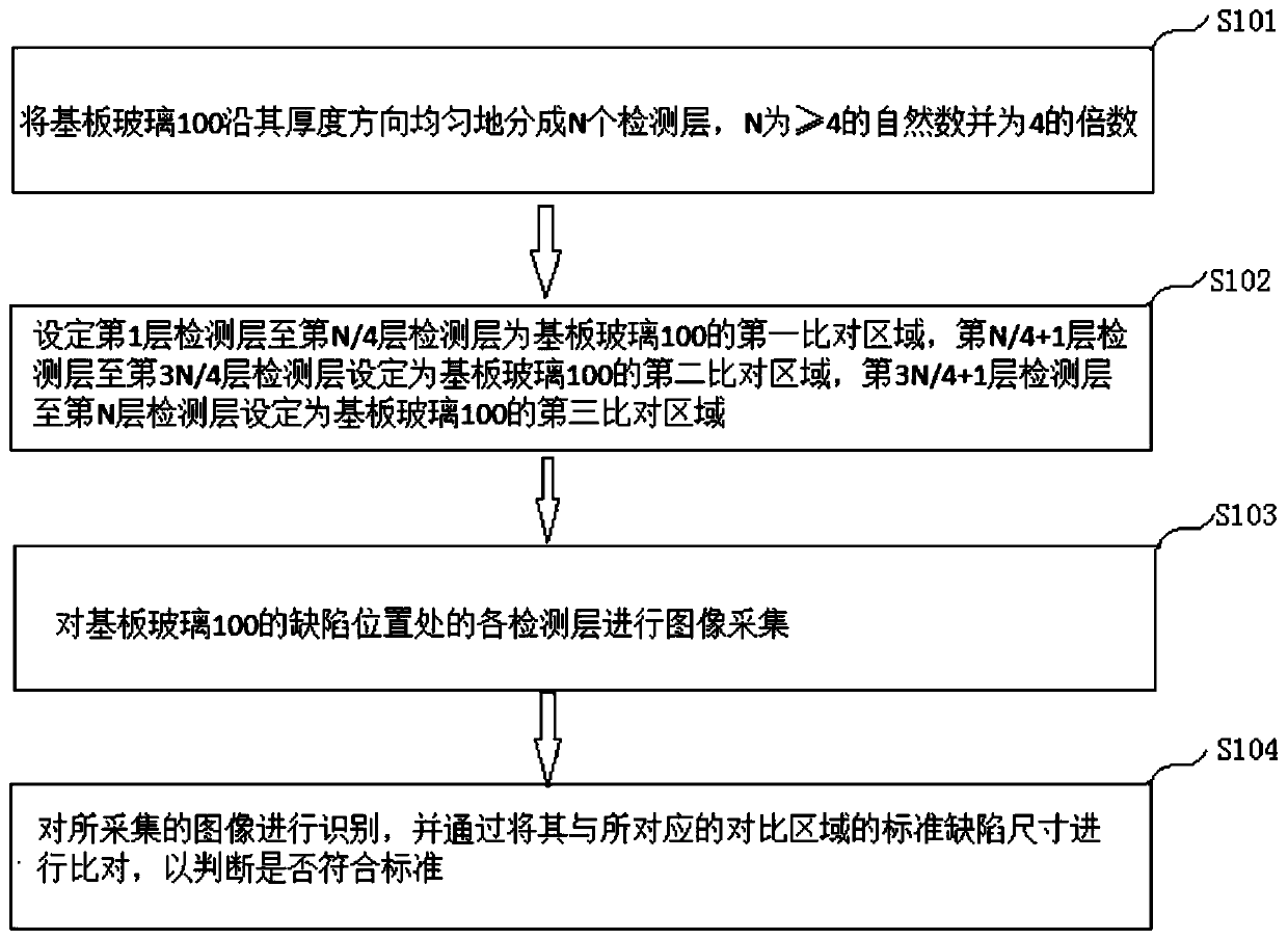
[0033] Such as figure 1 As shown, the present disclosure provides a substrate glass defect detection method for substrate glass defects. The steps of the substrate glass defect detection method include: S101, dividing the substrate glass 100 into N detection layers uniformly along its thickness direction, where N is a natural number ≥4 And is a multiple of 4; S102, set the detection layer from the first layer to the N/4th layer to the first comparison area of the substrate glass 100, and the detection layer from the N/4+1th layer to the 3N/4th layer to detect The layer is set as the second comparison area of the substrate glass 100, and the 3N/4+1 detection layer to the Nth detection layer are set as the third comparison area of the substrate glass 100; S103, the defect of the substrate glass 100 Image collection is performed on each detection layer at the position; S104, the collected image is recognized, and it is compared with the standard defect size of the corresponding contrast area to determine whether it meets the standard.
[0034] In the above technical solution, the substrate glass 100 is evenly divided into N detection layers along its thickness direction, and the first comparison area, the second comparison area, and the third comparison area are respectively set, and the defects of the substrate glass 100 Images are collected and identified for each detection layer at the location to compare the image of the layer with the standard defect size of the corresponding contrast area to determine whether it meets the standard. This detection method is convenient for judging whether the substrate glass is qualified and High detection accuracy.
[0035] Specifically, the image acquisition of each detection layer at the defect position of the substrate glass 100 includes: realizing the separate detection of the N detection layers through the zoom of the image acquisition device, which is convenient for the operation of the inspection personnel and has strong operability. For example, the image capture device may be a zoomable camera.
[0036] In one embodiment, the thickness of the substrate glass 100 may be 0.4 mm or 0.8 mm, and N is 4, or N is 8, or N is 16. When N is 4 and the thickness of the substrate glass 100 is 0.4mm, the substrate glass 100 is evenly divided into 4 layers with a change of 0.1mm. The first comparison area is the first detection layer, and the second comparison area It is the second detection layer and the third detection layer, and the third comparison area is the fourth detection layer; when N is 8 and the thickness of the substrate glass 100 is 0.4mm, the substrate glass 100 changes by 0.05 The amount is evenly divided into 8 layers, the first comparison area is the first detection layer and the second detection layer, the second comparison area is the third detection layer to the sixth detection layer, and the third comparison area is the seventh Layer detection layer and eighth layer detection layer. When N is 16 or other multiples of 4, it can also be divided by the above setting. In theory, the larger the N, the higher the accuracy of the substrate glass defect detection method.
[0037] In one embodiment, the standard defect size of the first comparison area is no more than 0.02mm, the standard defect size of the second comparison area is no more than 0.05mm, and the standard defect size of the third comparison area is no more than 0.1 mm, when the first comparison area, the second comparison area, and the third comparison area at the defect position of the substrate glass 100 meet their respective standards, the substrate glass 100 meets the qualified standard, but in the actual inspection process Among them, the defect usually only exists in a certain comparison area, and the standard defect size of the comparison area is met, and the substrate glass 100 meets the standard.
[0038] The present disclosure also provides a substrate glass defect detection device, which can perform defect detection on the substrate glass 100 according to the substrate glass defect detection method. The substrate glass detection device includes a control unit for imaging the defect position of the substrate glass 100 The captured zoomable camera unit; the camera unit includes a drive unit 21, a movable object side lens 22, a fixed camera unit body 23, and an image side lens 24 fixedly connected to the camera unit body 23. The drive unit 21 controls The control command sent by the unit drives the object-side lens 22 to move along its center line to achieve focusing and image collection on the N detection layers at the defect position; the control unit is used to identify the images collected by the camera unit, and through It is compared with the standard defect size of the corresponding comparison area to determine whether it meets the standard.
[0039] In the above technical solution, the detection device is provided with a zoomable camera unit and the drive section 21 drives the object side lens 22 to move along its center line according to the control command sent by the control unit, so as to realize N detections at the defect position. Layer focusing and image collection; the control unit is used to identify the image collected by the camera unit and compare it with the standard defect size of the corresponding contrast area to determine whether it meets the standard. The device can realize the detection, identification and judgment of substrate glass defects, with high detection accuracy and high degree of automation, without manual identification and judgment.
[0040] Optionally, the aforementioned control unit may be configured as an industrial computer.
[0041] Optionally, the driving part 21 may be configured as a linear motor, which has low cost and stable driving. However, the present disclosure does not limit the specific structure type of the driving part 21, and other types of driving structures can also be selected.
[0042] Optionally, the camera unit body 23 can be configured as a CCD matrix color camera, which has good imaging effect and is convenient for image collection. Of course, the present disclosure does not limit the specific structure type of the camera unit body 23.
[0043] In one embodiment, such as figure 2 As shown, the substrate glass defect detection device may further include a light source 4 for illuminating the defect position of the substrate glass 100. The center line of the light source 4 coincides with the center line of the object side lens 22 so that the light beam emitted by the light source 4 is The image acquisition path A of the camera unit is directed to the defect position, with good lighting effect and good imaging effect.
[0044] Specifically, the light source 4 uses LED light-emitting diodes to emit wavelengths between 400-800nm, beam divergence of 37°, and radiation area greater than 10mm 2 In order to ensure that the light beam emitted by the light source 4 is as parallel as possible to improve the lighting effect.
[0045] In other embodiments, the substrate glass defect detection device may further include a distance measuring unit 3. The distance measuring unit 3 is used to measure the distance between the detection device and the substrate glass 100, and the control unit is used to measure the distance between the detection device and the substrate glass 100. The distance information controls the camera unit to focus on the side of the substrate glass 100 close to the detection device at the defect position. In other words, the camera unit is focused on the reference surface (the side close to the detection device) of the substrate glass 100 through the distance measurement unit 3 to realize the automatic focusing of the detection device with a high degree of automation. Of course, it is also possible to manually focus on the reference plane, which is not limited in the present disclosure.
[0046] Further, the distance measuring unit 3 may include a laser emitter and a photoelectric receiver for receiving laser light emitted from the laser emitter and reflected by the substrate glass 100. For example, the laser transmitter can emit a laser with a wavelength of 650 nm, and the laser is a continuous wave with a power of less than 1 mW. After being reflected by the substrate glass 100 on the side of the detection device, the laser reaches the photoelectric receiver. The distance between the detection device and the reference surface is determined by detecting the time taken by the laser to emit from the laser transmitter and the photoelectric receiver to receive the laser. The measurement accuracy is high and the cost of components is low. In another embodiment, the distance measuring unit 3 may also be configured as an ultrasonic distance sensor, which is not limited in the present disclosure.
[0047] In addition, the camera unit may also include a first reflection mechanism 25 and a second reflection mechanism 26. The center line of the object side lens 22 is used to be parallel to the substrate glass 100, and the center line of the image side lens 24 is used to be perpendicular to the substrate glass 100. A reflection mechanism 25 is used to reflect the image information of the defect position to the object side lens 22, and the second reflection mechanism 26 is used to reflect the image information received by the object side lens 22 to the image side lens 24. The first reflection mechanism 25 and the second reflection mechanism 26 are provided to achieve image collection under the condition that the center line of the object side lens 22 and the center line of the image side lens 24 do not overlap, so that the object side lens 22 The specific arrangement of the image-side lens 24 is more flexible and facilitates the arrangement of the structure.
[0048] Further, the first reflection mechanism 25 and the second reflection mechanism 26 may be configured as a first right-angle prism and a second right-angle prism, respectively, and the slopes of the first and second right-angle prisms are configured as the first reflection surface 251 and The second reflection surface 261. The two right-angle prisms have low cost and good reflection effect.
[0049] Furthermore, the light source 4 is arranged adjacent to the right-angled surface of the second right-angled prism, so that the light beam emitted by the light source 4 passes through the second right-angled prism and the object side lens 22 in turn, and then is directed to the defect position through the first reflecting surface 251. When the light beam passes through the second right-angle prism, the light beam passes through the transparent right-angle prism in parallel without being refracted or reflected, but when the light beam passes through the object side lens 22 and is directed toward the first reflecting surface 251, the light beam will be reflected. Specifically, the incident angle of the light beam to the first reflective surface 251 is 45 degrees, so that the light beam can be directed perpendicularly to the defect position of the substrate glass 100 to achieve a good lighting effect.
[0050] Optionally, the above-mentioned object-side lens 22 may be configured as a convex lens, and the image-side lens 24 may be configured as a concave lens. The centers of curvature of the convex lens and the concave lens coincide, and the radius of curvature of the concave lens may be twice the radius of curvature of the convex lens. Further improve the imaging effect.
[0051] In addition, such as figure 2 As shown, the substrate glass defect detection device may further include a housing 10, and the control unit, the camera unit, etc. may all be arranged in the housing 10, so as to protect the components of the device through the housing 10.
[0052] The specific working process of the substrate glass defect detection device is as follows:
[0053] First, install the detection device at a distance of 4 cm to 8 cm from the substrate glass to ensure that the camera unit in the detection device can work normally;
[0054] Secondly, the control unit can first control the light source 4 to illuminate the defect position;
[0055] Furthermore, the control unit can control the distance measurement unit 3 to measure the distance between the detection device and the substrate glass 100. After the measurement is completed, the distance measurement unit 3 feeds back the distance information to the control unit, and the control unit performs an algorithm based on the distance information. Operate to control the camera unit to focus on the side of the substrate glass 100 that is close to the detection device. After the focusing is completed, the camera unit performs image capture on this side;
[0056] Then, the control unit sends a control command to the drive unit 21 to drive the object-side lens 22 to move along its center line to achieve N times of focusing on the substrate glass 100. The amount of change in each focus can be the same so that the camera unit can move along the Focus and shoot uniformly in the thickness direction of the substrate glass;
[0057] Finally, the camera unit feeds back multiple captured image information to the control unit, and the control unit compares the collected images and compares them with the standard defect size of the corresponding contrast area to determine the substrate glass Whether 100 meets the standard.
[0058] The preferred embodiments of the present disclosure are described in detail above with reference to the accompanying drawings. However, the present disclosure is not limited to the specific details in the above-mentioned embodiments. Within the scope of the technical concept of the present disclosure, various simple modifications can be made to the technical solutions of the present disclosure. These simple modifications all belong to the protection scope of the present disclosure.
[0059] In addition, it should be noted that the various specific technical features described in the above-mentioned specific embodiments can be combined in any suitable manner without contradiction. In order to avoid unnecessary repetition, the present disclosure provides various possible The combination method will not be explained separately.
[0060] In addition, various different embodiments of the present disclosure can also be combined arbitrarily, as long as they do not violate the idea of the present disclosure, they should also be regarded as the content disclosed in the present disclosure.
PUM
Property | Measurement | Unit |
Thickness | 0.4 ~ 0.8 | mm |
Description & Claims & Application Information
We can also present the details of the Description, Claims and Application information to help users get a comprehensive understanding of the technical details of the patent, such as background art, summary of invention, brief description of drawings, description of embodiments, and other original content. On the other hand, users can also determine the specific scope of protection of the technology through the list of claims; as well as understand the changes in the life cycle of the technology with the presentation of the patent timeline. Login to view more.