Patterning method, etching method, manufacturing method of display panel and display panel

A technology for display panels and graphics, which is applied in the fields of graphics, etching, display panels, and display panels. It can solve the problems of rough exposure edges, impermeable exposure, and unclean development, and achieve uniform and more thorough exposure and enhanced exposure. Strength, roughness improvement effect

Active Publication Date: 2020-06-05
HEFEI VISIONOX TECH CO LTD
View PDF9 Cites 0 Cited by
  • Summary
  • Abstract
  • Description
  • Claims
  • Application Information

AI Technical Summary

Problems solved by technology

see figure 1 , figure 1 It is a schematic diagram of the graphic method in the existing method. With the development of micro-manufacturing technology, the graphic structure to be produced is more precise, and the graphic gap in the dense area is getting smaller and smaller, and the problems of poor exposure and poor development often occur. Rough exposure edges, film residue, etc.

Method used


Image

  • Patterning method, etching method, manufacturing method of display panel and display panel
  • Patterning method, etching method, manufacturing method of display panel and display panel
  • Patterning method, etching method, manufacturing method of display panel and display panel

Examples


Embodiment Construction

[0021] In order to make the purpose, technical solution and effect of the present application more clear and definite, the present application will be further described in detail below with reference to the accompanying drawings and examples.

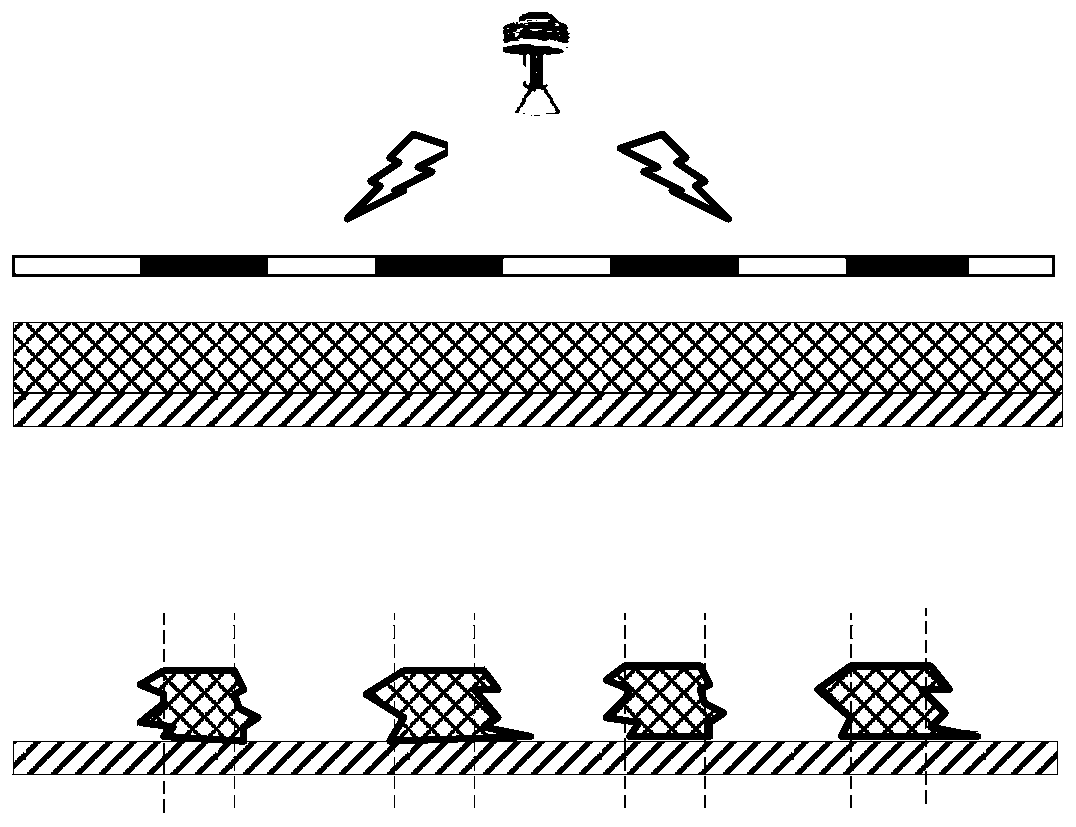
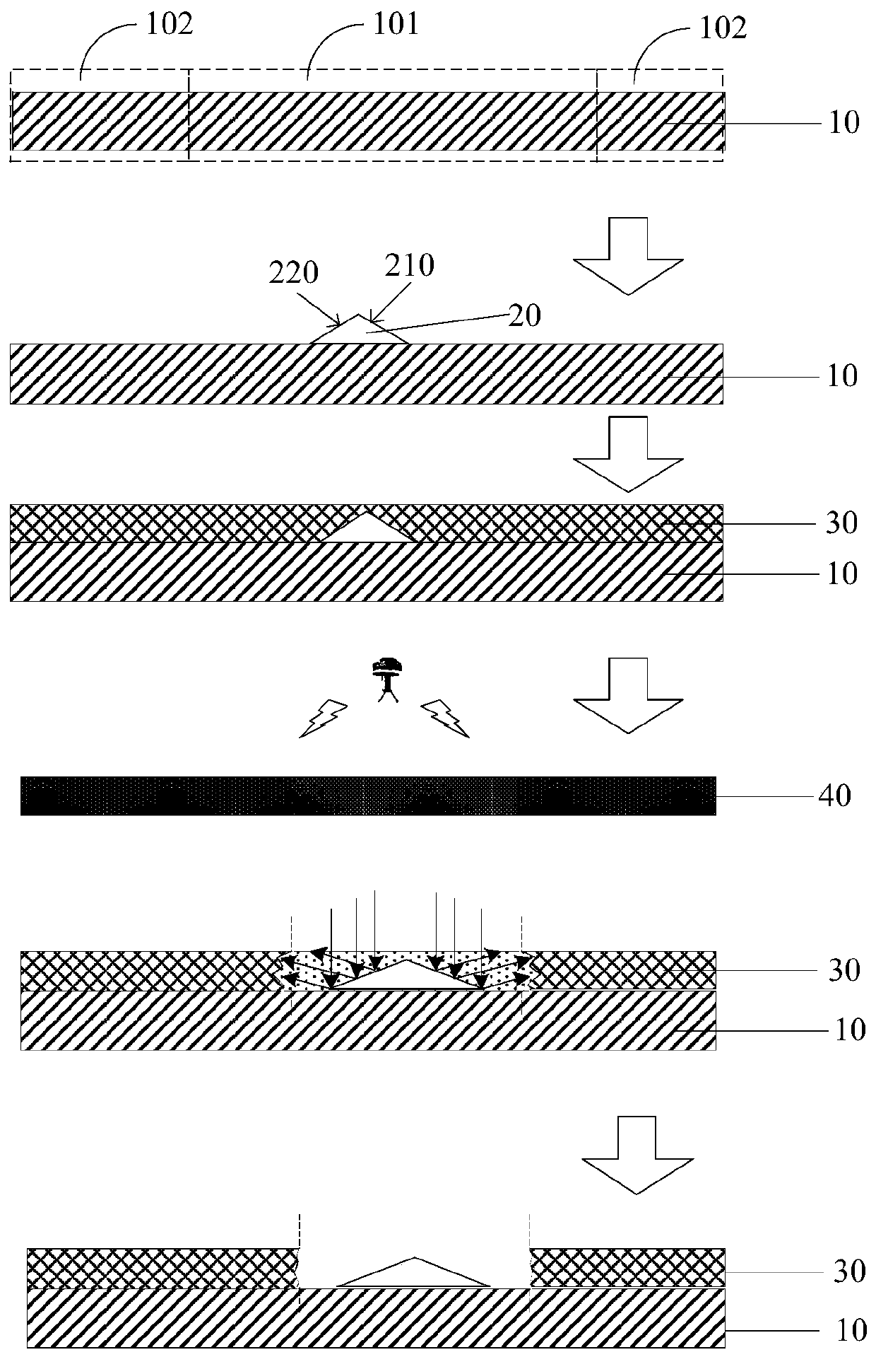
[0022] The present application provides a patterning method, which can improve the exposure accuracy of the photoresist layer. The method is realized by setting reflective blocks in the photoresist layer and using the reflective blocks to reflect exposure light in different directions.

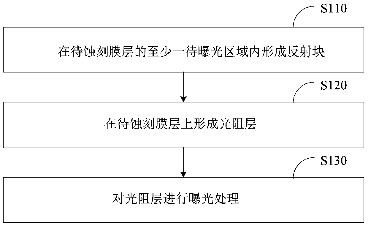
[0023] see figure 2 , figure 2 It is a schematic flowchart of the graphical method in the embodiment of the present application. In this embodiment, the graphical method includes:

[0024] S110: Form a reflective block in at least one area to be exposed of the film layer to be etched.

[0025] S120: forming a photoresist layer on the film layer to be etched.

[0026] Wherein, the photoresist layer covers the film layer to be etched and wraps the r...


PUM

PropertyMeasurementUnit
widthaaaaaaaaaa

Abstract

The invention discloses a patterning method, an etching method, a manufacturing method of a display panel and the display panel. The patterning method comprises: forming a reflection block in at leastone to-be-exposed area of a to-be-etched film layer; forming a photoresist layer on the to-be-etched film layer, wherein the photoresist layer covers the to-be-etched film layer and wraps the reflection block at the same time; and performing exposure processing on the photoresist layer, wherein the surface of the reflection block at least comprises two reflection areas with different light emitting directions, and the reflection areas are used for reflecting incident light in the same direction to the photoresist layer in different directions. In this way, the exposure precision can be improved.

Description

technical field [0001] The present application relates to the field of display technology, in particular to patterning, etching, a method for manufacturing a display panel and a display panel. Background technique [0002] Etching (Etch) is a technology that removes materials by means of chemical reaction or physical impact, and is often used in semiconductor manufacturing processes. Generally, the pattern is transferred to the dielectric layer through exposure, plate making and development, and then the part to be removed is etched by chemical solution or ion impact. see figure 1 , figure 1 It is a schematic diagram of the graphic method in the existing method. With the development of micro-manufacturing technology, the graphic structure to be produced is more precise, and the graphic gap in the dense area is getting smaller and smaller, and the problems of poor exposure and poor development often occur. Causes exposure edge roughness, film residue, etc. With the contin...

Claims


Application Information

Patent Timeline
Patent Type & Authority Applications(China)
IPC IPC(8): H01L21/027G03F7/00
CPCH01L21/0274G03F7/0035
Inventor 张波王中来刘晓佳李柯王瑞瑞杨大伟
Owner HEFEI VISIONOX TECH CO LTD
Why Eureka
Try Eureka