
led manufacturing process

A preparation process and pressure technology, which is applied in the field of LED preparation process, can solve the problems of unsatisfactory LED performance and difficulty in meeting customer requirements, and achieve the effects of reducing the risk of splitting, reducing interface stress, and increasing growth rate

Active Publication Date: 2021-05-18
江西通利晟电子科技有限公司
View PDF3 Cites 0 Cited by
  • Summary
  • Abstract
  • Description
  • Claims
  • Application Information

AI Technical Summary

Problems solved by technology

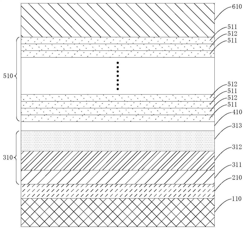
The light-emitting layer is generally composed of periodically stacked light-emitting well layers and light-emitting barrier layers. The light-emitting well layer forms indium gallium nitride by doping indium in the gallium nitride layer, and the light-emitting barrier layer is a gallium nitride layer. Many deficiencies make the performance of the produced LED not ideal enough to meet customer requirements

Method used


Image

  • led manufacturing process
  • led manufacturing process

Examples


Embodiment Construction

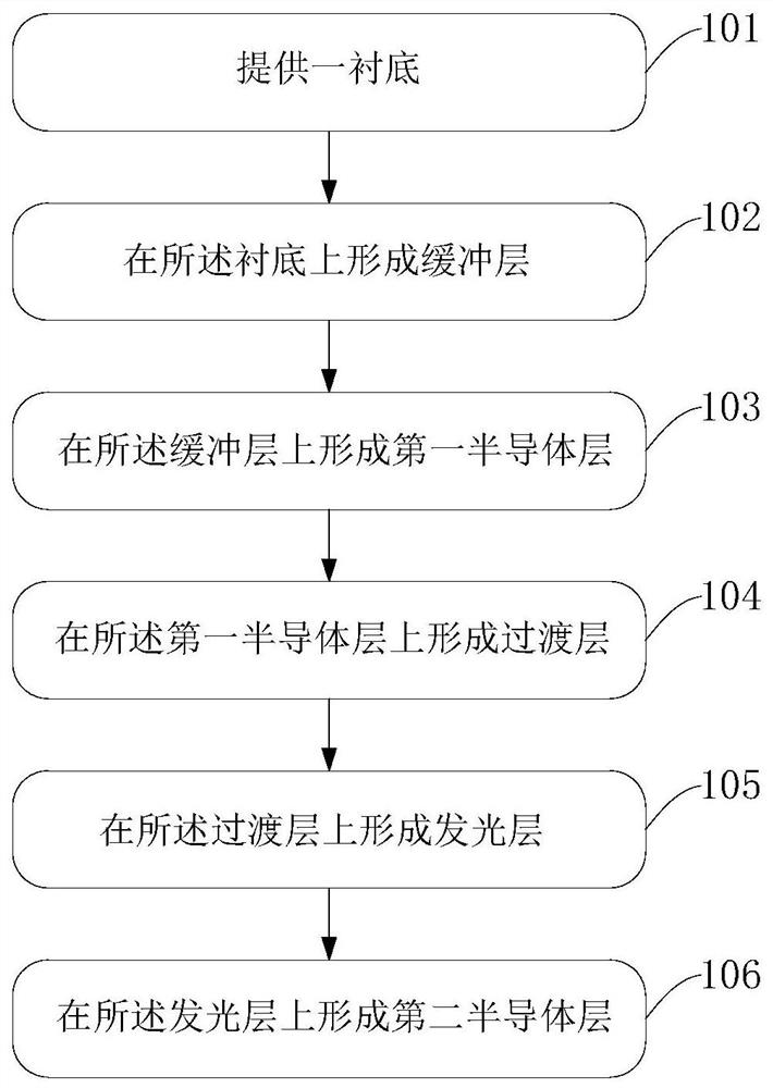
[0027] The LED manufacturing process provided by the present invention will be described in more detail below in conjunction with the accompanying drawings, wherein a preferred embodiment of the present invention is represented, it should be understood that those skilled in the art can modify the present invention described here, and still realize the advantages of the present invention Effect. Therefore, the following description should be understood as the broad knowledge of those skilled in the art, but not as a limitation of the present invention.

[0028] In the following paragraphs the invention is described more specifically by way of example with reference to the accompanying drawings. Advantages and features of the present invention will be apparent from the following description and claims. It should be noted that all the drawings are in a very simplified form and use imprecise scales, and are only used to facilitate and clearly assist the purpose of illustrating th...


PUM

PropertyMeasurementUnit
thicknessaaaaaaaaaa

Abstract

The present invention provides an LED manufacturing process, comprising providing a substrate, sequentially forming a buffer layer, a first semiconductor layer, a transition layer, a light-emitting layer, and a second semiconductor layer on the substrate; forming the first semiconductor layer During the process, the pressure of the reaction chamber is maintained at the first pressure, and during the process of forming the light-emitting layer, the pressure of the reaction chamber is maintained at the second pressure, and the second pressure is lower than the first pressure. During the formation of the transition layer, the pressure of the reaction chamber is The starting pressure of the body is equal to the first pressure, and the ending pressure is equal to the second pressure. In the present invention, by introducing a transition layer between the first semiconductor layer and the light-emitting layer, the continuous growth is maintained during the pressure change process at this stage, and the interfacial stress is reduced through the transition layer, so that the growth of the first semiconductor layer under high pressure conditions can be realized, and the growth rate can be increased. , due to the gradual reduction of pressure during the formation of the transition layer, the surface tensile stress of the first semiconductor layer gradually decreases, reducing the risk of cracks in the process.

Description

technical field [0001] The invention relates to the technical field of semiconductors, in particular to an LED preparation process. Background technique [0002] LED (Lighting Emitting Diode) lighting is light-emitting diode lighting, which is a semiconductor solid-state light-emitting device. It uses a solid semiconductor chip as a light-emitting material. In the semiconductor, the excess energy is released through the recombination of carriers to cause photon emission, and directly emits red, yellow, blue, and green light. On this basis, using the principle of three primary colors, Adding fluorescent powder can emit light of any color. The lighting fixtures manufactured using LEDs as light sources are LED lamps. [0003] The LED manufacturing process is divided into epitaxy, chip front-end, chip back-end, packaging and other links. The epitaxy is sequentially deposited on the sapphire substrate through the metal-organic chemical vapor deposition process. structure, and ...

Claims


Application Information

Patent Timeline
Patent Type & Authority Patents(China)
IPC IPC(8): H01L33/00H01L33/12
CPCH01L33/007H01L33/12
Inventor 孙蕾蕾
Owner 江西通利晟电子科技有限公司
Learn More