A Method for Adjusting Beam Divergence Angle of Vertical Cavity Surface Emitting Semiconductor Laser

A technology of vertical cavity surface emission and beam divergence angle, applied in semiconductor lasers, lasers, laser parts and other directions, can solve the problems of current density affecting the reliability of VCSELs, light-emitting area limiting the maximum output power of VCSELs, etc.

Active Publication Date: 2021-09-10
江西德瑞光电技术有限责任公司
View PDF13 Cites 0 Cited by
  • Summary
  • Abstract
  • Description
  • Claims
  • Application Information

AI Technical Summary

Problems solved by technology

But for smaller oxidation holes, the reduced light-emitting area limits the maximum output power of VCSEL, and at the same time, the high current density also affects the reliability of VCSEL

Method used


Image

  • A Method for Adjusting Beam Divergence Angle of Vertical Cavity Surface Emitting Semiconductor Laser
  • A Method for Adjusting Beam Divergence Angle of Vertical Cavity Surface Emitting Semiconductor Laser

Examples


Embodiment Construction

[0015] The implementation of the present invention will be described in detail below with reference to the drawings and examples, so as to fully understand and implement the implementation process of how to use technical means to solve technical problems and achieve technical effects in the present invention.

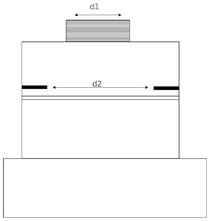
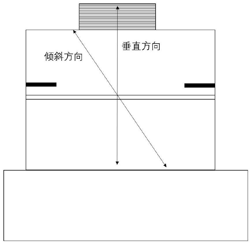
[0016] A method for adjusting the beam divergence angle of a vertical cavity surface-emitting semiconductor laser, using epitaxial technology to sequentially grow an N-type semiconductor reflective layer, an active layer, and a P-type semiconductor reflective layer on a semiconductor substrate; the N-type semiconductor reflective layer and the P The type semiconductor reflection layer is a plurality of pairs of distributed Bragg mirror layers composed of two semiconductor materials with different refractive indices;

[0017] The P-type semiconductor DBR has a reduced logarithm;

[0018] A certain logarithm of the dielectric DBR layer is fabricated on the P-type semicond...


PUM

PropertyMeasurementUnit
sizeaaaaaaaaaa

Abstract

The invention discloses a method for adjusting the beam divergence angle of a vertical cavity surface-emitting semiconductor laser. An N-type semiconductor reflection layer, an active layer, and a P-type semiconductor reflection layer are sequentially grown on a semiconductor substrate by using epitaxial technology; the N-type semiconductor The reflective layer and the P-type semiconductor reflective layer are multiple pairs of distributed Bragg mirror layers composed of two semiconductor materials with different refractive indices; the P-type semiconductor DBR has a reduced logarithm; it is fabricated on the P-type semiconductor reflective layer A certain logarithm of the dielectric DBR layer; the divergence angle of the VCSEL is adjusted by adjusting the lateral dimension of the dielectric DBR layer. The invention can realize the adjustment of the divergence angle of the VCSEL on the basis of maintaining a larger diameter of the oxidation hole.

Description

technical field [0001] The invention relates to the technical field of semiconductor lasers, in particular to a method for adjusting the beam divergence angle of a vertical cavity surface emitting semiconductor laser. Background technique [0002] A vertical cavity surface emitting laser is a type of semiconductor laser. A conventional VCSEL forms a VCSEL by sequentially forming a first mirror layer, an active layer, and a second mirror layer on a substrate material. The first and second reflector layers are distributed Bragg reflector (DBR) semiconductor layers formed by alternating high and low refractive index materials. Taking GaAs-based VCSEL as an example, the substrate material is generally N-type GaAs material, the first mirror is an N-type semiconductor layer of AlxGa1-xAs with two different Al compositions, the active layer is a multi-quantum well structure, and the second The mirror layer is an AlxGa1-xAs N-type semiconductor layer with two different Al compositi...

Claims


Application Information

Patent Timeline
Patent Type & Authority Patents(China)
IPC IPC(8): H01S5/183
CPCH01S5/183H01S5/18361H01S5/18377
Inventor 徐化勇仇伯仓高阳蒋锴
Owner 江西德瑞光电技术有限责任公司
Why Eureka
Try Eureka