Photoelectric conversion element and method for manufacturing same
A technology of photoelectric conversion elements and manufacturing methods, which is applied in the fields of electrical components, semiconductor/solid-state device manufacturing, photovoltaic power generation, etc., can solve the problems of weak current flow and lower precision, and achieve the effect of improving the specific detection rate
- Summary
- Abstract
- Description
- Claims
- Application Information
AI Technical Summary
Problems solved by technology
Method used
Image
Examples
preparation example Construction
[0283] (preparation of ink)
[0284] Inks can be prepared by known methods. For example, it can be prepared by the following method: mixing the first solvent and the second solvent to prepare a mixed solvent, adding a p-type semiconductor material and an n-type semiconductor material to the mixed solvent; adding a p-type semiconductor material to the first solvent , a method of adding an n-type semiconductor material to a second solvent, and then mixing the first solvent and the second solvent to which each material is added; and the like.
[0285] The first solvent and the second solvent, and the p-type semiconductor material and n-type semiconductor material can be mixed by heating at a temperature not higher than the boiling point of the solvent.
[0286] After mixing the first solvent and the second solvent, and the p-type semiconductor material and n-type semiconductor material, the resulting mixture can be filtered using a filter, and the obtained filtrate can be used a...
Embodiment 1
[0301] (Production and evaluation of photoelectric conversion elements)
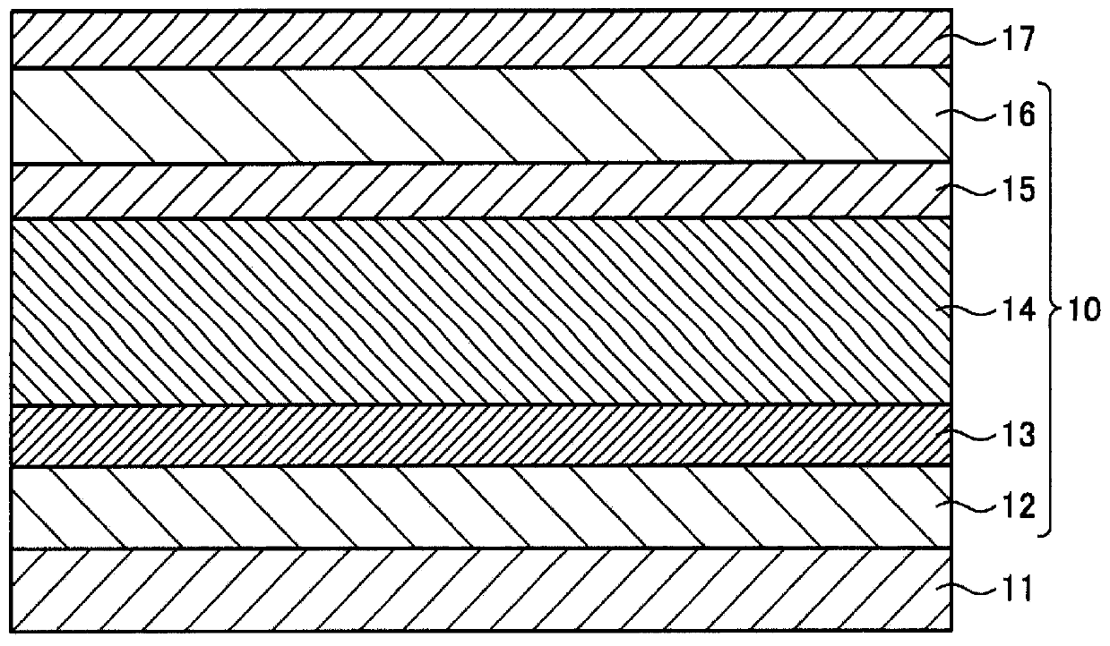
[0302] A glass substrate on which an ITO thin film (anode) was formed to a thickness of 150 nm by a sputtering method was prepared, and ozone UV treatment was performed on this glass substrate as a surface treatment.
[0303] Next, poly(3,4-ethylenedioxythiophene) and polystyrene sulfonic acid (PEDOT / PSS) were dissolved in water, and the resulting suspension (Clevios P VP AI4083, manufactured by Heraeus) was prepared using a pore size of 0.45 μm filter for filtration. The filtered suspension was applied to a thin film of ITO on a glass substrate with a thickness of 40 nm by a spin coating method to form a coating film.
[0304] Next, the glass substrate on which the coating film was formed was dried at 200° C. for 10 minutes using a hot plate in the atmosphere to form a hole transport layer.
[0305] Next, polymer P-1 and C60PCBM (manufactured by Frontier Carbon, trade name: E100) were mixed at a weigh...
Embodiment 2~4 and comparative example 1~5
[0317] Except for changing the thickness of the active layer as shown in Table 3 below, a photoelectric conversion element (photodetection element) was fabricated in the same manner as in Example 1 described above, and evaluated in the same manner as in Example 1. The results are shown in Table 3.
[0318] [table 3]
[0319]
[0320] D* of the photoelectric conversion elements of Examples 1 to 4 was higher than that of the photoelectric conversion elements of Comparative Examples 1 to 5 in which the absorption peak wavelength of the p-type semiconductor material was less than 800 nm and the thickness condition of the active layer was not satisfied.
[0321] That is, EQE generally has a tendency to decrease as the absorption peak wavelength of the p-type semiconductor material increases, but according to the photoelectric conversion elements of Examples 1 to 4, by making the thickness of the active layer 350nm to 500nm, making the p-type semiconductor material The absorptio...
PUM
| Property | Measurement | Unit |
|---|---|---|
| thickness | aaaaa | aaaaa |
| wavelength | aaaaa | aaaaa |
| thickness | aaaaa | aaaaa |
Abstract
Description
Claims
Application Information


