
Indium selenide photoelectric detector using stannous selenide nanocrystals for surface modification, and preparation method thereof

A technology of photodetector and tin selenide, applied in the field of photoelectric detection

Active Publication Date: 2021-08-31
SHENZHEN UNIV
View PDF7 Cites 0 Cited by
  • Summary
  • Abstract
  • Description
  • Claims
  • Application Information

AI Technical Summary

Problems solved by technology

However, there are few reports in the prior art on the use of nanocrystal-modified InSe photodetectors

Method used


Image

  • Indium selenide photoelectric detector using stannous selenide nanocrystals for surface modification, and preparation method thereof
  • Indium selenide photoelectric detector using stannous selenide nanocrystals for surface modification, and preparation method thereof
  • Indium selenide photoelectric detector using stannous selenide nanocrystals for surface modification, and preparation method thereof

Examples


Embodiment 1

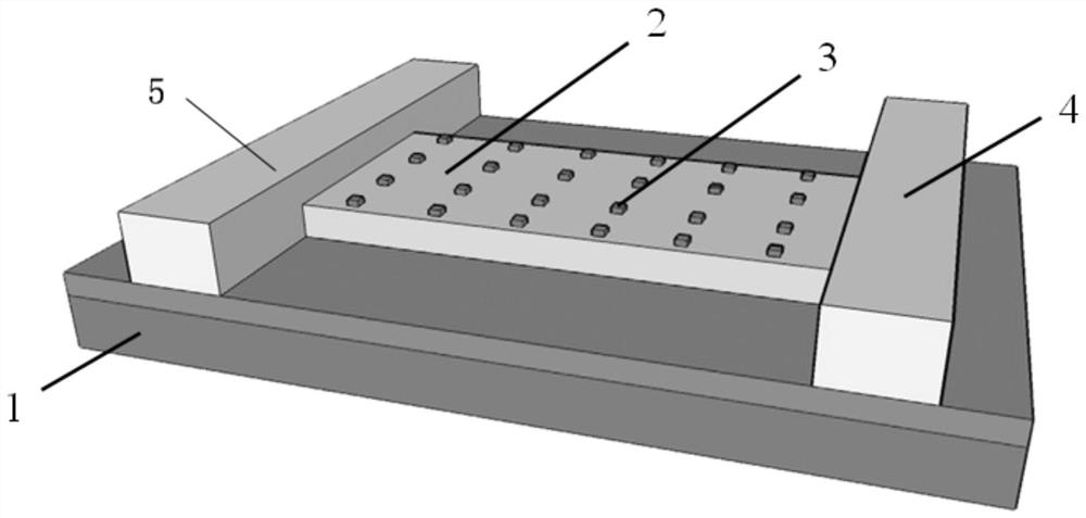
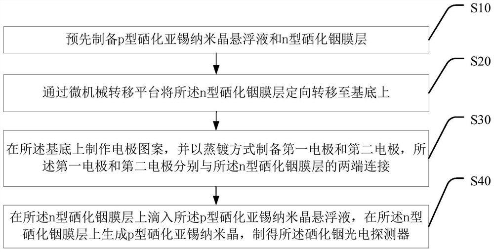
[0056] Preparation method of indium selenide photodetector surface modified by using tin selenide nanocrystals:

[0057] The p-type tin selenide nanocrystals were prepared by the liquid phase exfoliation method, and the n-type indium selenide thin layer was prepared by the mechanical exfoliation method. After that, the SiO 2 / Si substrate was cleaned and dried with nitrogen, and the n-type indium selenide flake layer was transferred to the PDMS substrate, and the n-type indium selenide flake layer on the PDMS substrate was transferred to the SiO 2 / Si substrate surface, further, using standard photolithography process on SiO 2 / Si substrate to make electrode patterns, and prepare gold electrodes on both ends of the n-type indium selenide thin layer by evaporation, and then use organic solvents to remove the photoresist and excess gold powder remaining in the photolithography process, Then, the p-type tin selenide nanocrystals are modified to the surface of the n-type indium s...


PUM

PropertyMeasurementUnit
thicknessaaaaaaaaaa
thicknessaaaaaaaaaa
thicknessaaaaaaaaaa

Abstract

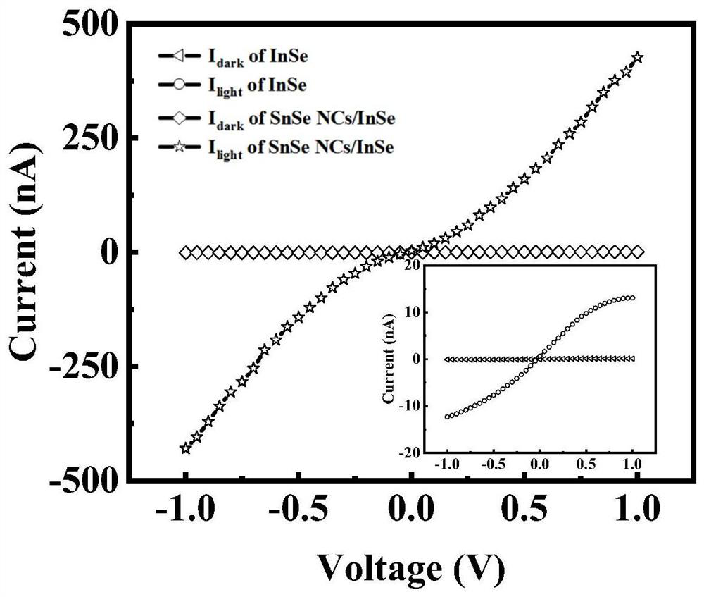
The invention discloses an indium selenide photoelectric detector using stannous selenide nanocrystals for surface modification, and a preparation method thereof. The indium selenide photoelectric detector comprises a substrate, an n-type indium selenide film layer arranged on the substrate, p-type stannous selenide nanocrystals arranged on the n-type indium selenide film layer, and a first electrode and a second electrode which are arranged on the substrate and connected with the two ends of the n-type indium selenide film layer respectively. On the premise that the microstructure of the indium selenide film layer is not changed, the p-type stannous selenide nanocrystalline is modified on the surface of the indium selenide film layer to form a local heterojunction, under illumination, the heterojunction can enable the interface of the n-type indium selenide film layer and the p-type stannous selenide nanocrystalline to generate a large number of electrons and holes, and photo-induced electron holes can be quickly separated at the heterojunction formed by the stannous selenide nanocrystals and the indium selenide film layer, so that the light-dark current ratio, the light responsivity and the specific detection rate of the prepared photoelectric detector can be effectively improved.

Description

technical field [0001] The invention relates to the field of photoelectric detection, in particular to an indium selenide photodetector surface-modified by tin selenide nanocrystals and a preparation method thereof. Background technique [0002] A photodetector is a photodetection device made using the photoconductive effect of semiconductor materials. Semiconductor photodetectors can cause changes in electrical properties by exciting non-equilibrium carriers in semiconductor materials through photons, which have the characteristics of small size, integration, fast response speed and high sensitivity. Photodetectors are widely used, covering various fields of military and national economy, and promote the development of aerospace, night vision and medical imaging, solar cells, wide-spectrum switches, optical communications, biometrics and other fields. At present, high-efficiency photodetectors formed by new two-dimensional material semiconductors are developing rapidly in ...

Claims


Application Information

Patent Timeline
Patent Type & Authority Applications(China)
IPC IPC(8): H01L31/101H01L31/032H01L31/0216H01L31/0352H01L31/18
CPCH01L31/101H01L31/0216H01L31/032H01L31/035227H01L31/18Y02P70/50
Inventor 李煜晏雨发郑博方曾海飞
Owner SHENZHEN UNIV
Learn More