Graphene/C60 composite film ultraviolet detector and preparation method thereof
A graphene and C60 technology, applied in the field of ultraviolet light detection, can solve difficult problems such as high responsivity and response speed, aging acceleration, etc., and achieve the effect of self-assembly coupling, strong light absorption, and photocurrent detection
- Summary
- Abstract
- Description
- Claims
- Application Information
AI Technical Summary
Problems solved by technology
Method used
Image
Examples
Embodiment 1
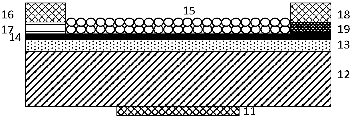
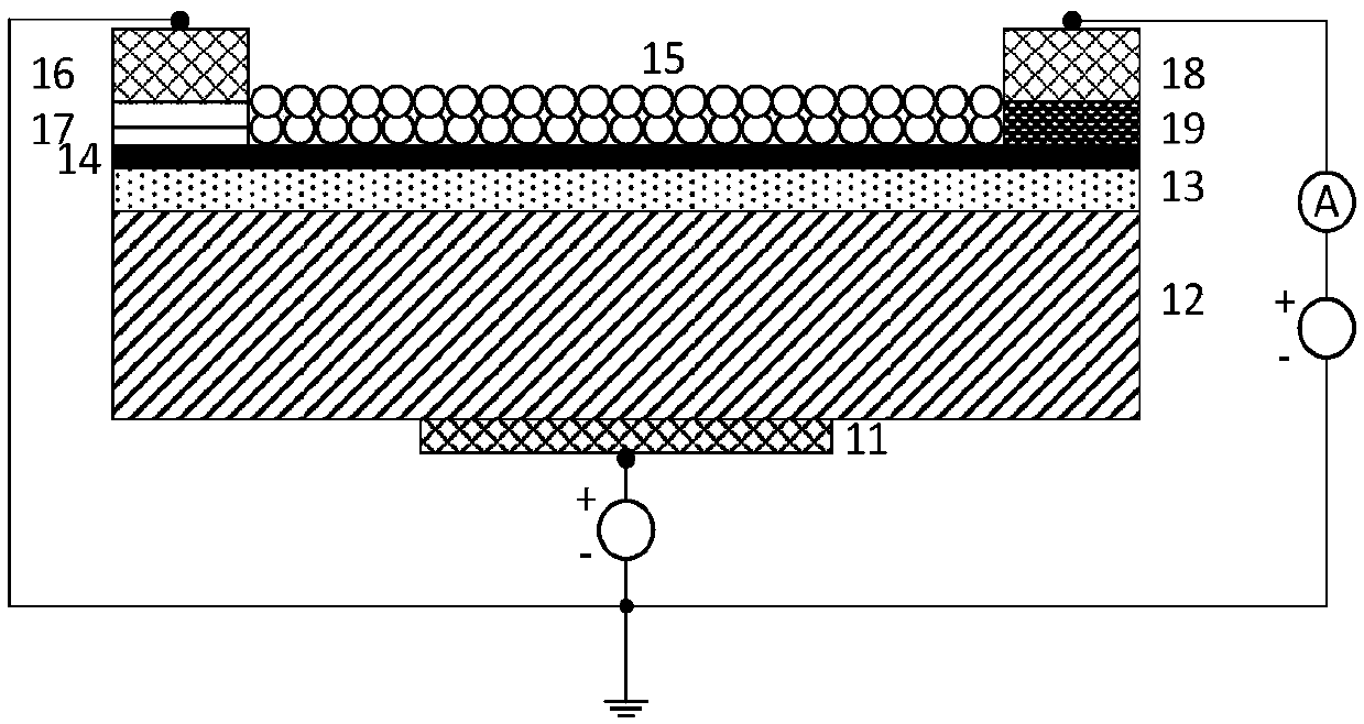
[0035] Embodiment 1: This embodiment provides a kind of based on graphene / C 60 The ultraviolet light detection transistor with composite absorption layer, the schematic diagram of its longitudinal section is shown in figure 1 shown.
[0036] A single ultraviolet light detection transistor includes a gate metal layer 11, a highly doped silicon gate 12 (0.5mm), a gate dielectric layer 13, a graphene / C 60 Composite absorbent layer.
[0037] Highly doped silicon gate 12 and gate dielectric layer 13 can simultaneously support graphene / C 60 Composite absorber thin film acts as the substrate of the whole transistor device.
[0038] Graphene / C 60 Composite absorber layer includes graphene layer 14 and C 60 Layer 15 (2-300nm).
[0039] The graphene layer 14 is in contact with the gate dielectric layer 13, and a source and a drain are formed at both ends; the source includes an upper source metal layer 16 and a lower source metal layer 17, and the drain metal layer includes an upp...
Embodiment 2
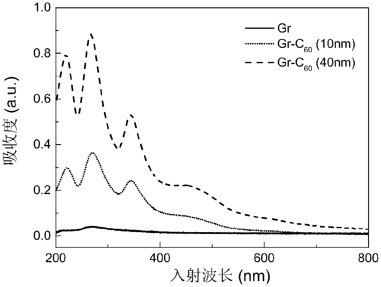
[0047] Embodiment 2: This embodiment provides a C-based 60 Thickness controllable graphene / C with controllable responsivity 60 Ultraviolet light detection transistor with composite absorbing layer. like image 3 As shown, different thicknesses of C were deposited on the graphene surface using the organic thermal evaporation method 60 Thin films, composite absorbing layers with different light absorbing degrees can be obtained. By controlling the thickness of C60, the ultraviolet absorption can be precisely controlled, so as to adjust the parameters such as quantum efficiency and responsivity of the device.
Embodiment 3
[0048] Embodiment 3: This embodiment provides based on graphene / C 60 Design scheme of m×n array composed of ultraviolet light detection transistors with composite absorbing layer. like Figure 4 As shown, the above is based on graphene / C 60 The gate of the ultraviolet light detection transistor 41 of the composite absorption layer is connected to the gate control terminal 41 through the protection resistor 43, and the drain is connected to the bit line 44 through the protection resistor 42, and the channel resistance value can be read out through the signal processing circuit. The ultraviolet light detection transistor array includes a plurality of ultraviolet light detection transistors 41 and related components constructed by m rows and n columns distributed in the array, and the resistance values in all transistors in the array are sequentially read through the peripheral signal processing circuit to perform optical signal or graphic information detection and identifica...
PUM
| Property | Measurement | Unit |
|---|---|---|
| Thickness | aaaaa | aaaaa |
| Thickness | aaaaa | aaaaa |
| Thickness | aaaaa | aaaaa |
Abstract
Description
Claims
Application Information


