
Preparation method of organic photoelectric detector and prepared organic photoelectric detector

A photodetector, organic technology, applied in photovoltaic power generation, electric solid state device, semiconductor/solid state device manufacturing, etc., can solve the problem of device photoelectric responsivity and EQE reduction, photogenerated carriers cannot be effectively extracted, and reduce device ratio detection. rate and other issues, to achieve the effect of optimizing internal configuration, realizing dark current and light response performance, and ensuring quality stability and reliability

Inactive Publication Date: 2021-08-17
UNIV OF ELECTRONIC SCI & TECH OF CHINA
View PDF8 Cites 0 Cited by
  • Summary
  • Abstract
  • Description
  • Claims
  • Application Information

AI Technical Summary

Problems solved by technology

However, when the thickness of the active layer is too large, generally around 500nm, the photoresponse of the device will drop sharply, and the photogenerated carriers cannot be effectively extracted, resulting in a decrease in the photoelectric responsivity and EQE of the device, thereby reducing the specific detectivity D of the device. *

Method used


Image

  • Preparation method of organic photoelectric detector and prepared organic photoelectric detector
  • Preparation method of organic photoelectric detector and prepared organic photoelectric detector
  • Preparation method of organic photoelectric detector and prepared organic photoelectric detector

Examples


preparation example Construction

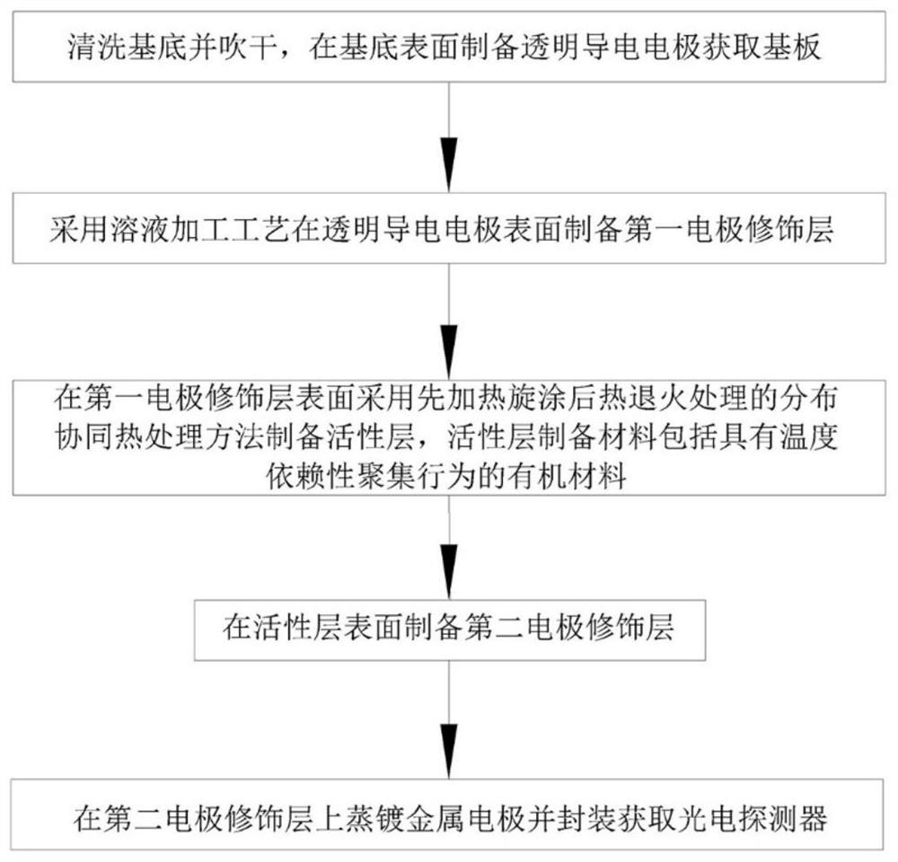
[0031] A method for preparing an organic photodetector, such as figure 1 shown, including

[0032] Clean the substrate and dry it, and prepare a transparent conductive electrode on the surface of the substrate to obtain the substrate;

[0033] preparing a first electrode modification layer on the surface of the transparent conductive electrode by using a solution processing technique;

[0034] On the surface of the first electrode modification layer, the active layer is prepared by a distributed synergistic heat treatment method of first heating, spin coating and then thermal annealing, and the preparation material of the active layer includes an organic material with temperature-dependent aggregation behavior;

[0035] preparing a second electrode modification layer on the surface of the active layer;

[0036] A metal electrode is vapor-deposited on the second electrode modification layer, and a photodetector is obtained by packaging.

[0037] An organic photodetector prep...

Embodiment 1

[0040] A method for preparing an organic photodetector. The prepared organic photodetector adopts an inverse structure. The preparation method specifically includes the following steps:

[0041] S01, cleaning the substrate and drying it with nitrogen gas after cleaning.

[0042] S02. Prepare a transparent conductive cathode on the surface of the substrate by magnetron sputtering, thermal evaporation, electron beam evaporation, spin coating, screen printing, spray coating or scrape coating, and then clean it with ultraviolet ozone.

[0043] Wherein, the substrate is glass or a transparent flexible substrate, and the transparent conductive cathode is an ITO film or FTO film. In this embodiment, the transparent conductive cathode ITO is used as an example for illustration, and the substrate and the transparent conductive cathode together constitute an ITO conductive glass.

[0044] S03. Prepare a cathode modification layer on the surface of the transparent conductive cathode by o...

Embodiment 2

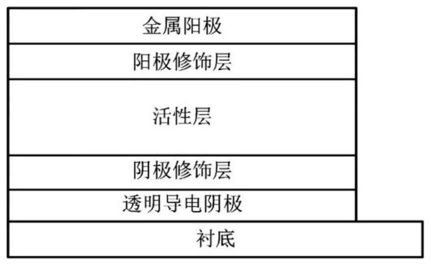
[0058] The difference between this embodiment and the first embodiment is that the prepared organic photodetector adopts a positive structure. The preparation method of organic photodetector comprises:

[0059] S01, cleaning the substrate and drying it with nitrogen gas after cleaning.

[0060] S02. Prepare a transparent conductive anode on the surface of the substrate by magnetron sputtering, thermal evaporation, electron beam evaporation, spin coating, screen printing, spray coating or scrape coating, and then clean it with ultraviolet ozone.

[0061] The transparent conductive anode is an ITO film or FTO film, and the substrate and the transparent conductive anode together form an ITO conductive glass.

[0062] S03. Prepare an anodic modification layer on the surface of the transparent conductive anode by using a solution processing technology of spin coating, screen printing, spray coating and scraping coating. The material of the anode modification layer is poly-TPD, PVK...


PUM

PropertyMeasurementUnit
Thicknessaaaaaaaaaa
Thicknessaaaaaaaaaa
Thicknessaaaaaaaaaa

Abstract

The invention discloses a preparation method of an organic photoelectric detector and the prepared organic photoelectric detector. The preparation method comprises the steps of firstly preparing a transparent conductive electrode, then preparing a first electrode modification layer, and then preparing an active layer by adopting an active layer solution of an organic material with a temperature-dependent aggregation behavior. The preparation process of the active layer adopts a distribution synergistic heat treatment method of heating spin coating firstly and then thermal annealing treatment, then a second electrode modification layer is prepared, and finally a metal electrode is evaporated and packaged to obtain the photoelectric detector. The organic photoelectric detector comprises a substrate, the transparent conductive electrode, the first electrode modification layer, the active layer, the second electrode modification layer and the metal electrode which are arranged from bottom to top. According to the present invention, the phase separation scale of the active layer can be regulated and controlled, the internal configuration of the active layer can be optimized, the low dark current density of a thick film device is kept, the light response rate and the external quantum efficiency EQE of the device are improved, and the specific detection rate D* of the device is further improved.

Description

technical field [0001] The invention belongs to the technical field of organic semiconductors, and in particular relates to a method for preparing an organic photodetector and the prepared organic photodetector. Background technique [0002] Photodetectors refer to devices that can convert optical signals into electrical signals, and are widely used in various fields such as military, aerospace, biomedicine, optical communication, and image sensing. Traditional inorganic photodetectors have poor mechanical flexibility, complicated preparation process and high price, which limit the development of photodetectors in the direction of large area, flexibility, high sensitivity and low cost. The characteristics of rich variety, excellent mechanical flexibility, solution processability and adjustable spectral absorption characteristics have greatly made up for the shortage of inorganic optoelectronic materials, making them have great research space and market value. [0003] Dark ...

Claims


Application Information

Patent Timeline
IPC IPC(8): H01L51/48H01L51/42
CPCH10K71/12H10K71/40H10K30/00Y02E10/549
Inventor 王洋刘青霞蒋亚东太惠玲袁柳肖建花
Owner UNIV OF ELECTRONIC SCI & TECH OF CHINA
Learn More