Class II superlattice infrared detector with broadband absorption enhancement structure and preparation method thereof

An infrared detector and enhanced structure technology, which is applied to semiconductor devices, electrical components, circuits, etc., can solve the problems of narrowing spectral response, limited application scenarios, and high device manufacturing costs, and can improve specific detection rate, reduce dark current, The effect of increasing the absorption rate

Pending Publication Date: 2022-04-19
CHONGQING INST OF GREEN & INTELLIGENT TECH CHINESE ACADEMY OF SCI
View PDF0 Cites 0 Cited by
  • Summary
  • Abstract
  • Description
  • Claims
  • Application Information

AI Technical Summary

Problems solved by technology

However, in order to obtain higher photoresponse intensity, the commonly used type II superlattice infrared detectors now require a micron-level thick absorbing layer, and the structure of the current plasma-enhanced infrared detector will lead to narrowing of the spectral response.
Thick absorbing layer and narrow spectral response bandwidth will lead to high manufacturing cost of the device and limited application scenarios

Method used


Image

  • Class II superlattice infrared detector with broadband absorption enhancement structure and preparation method thereof
  • Class II superlattice infrared detector with broadband absorption enhancement structure and preparation method thereof
  • Class II superlattice infrared detector with broadband absorption enhancement structure and preparation method thereof

Examples


Embodiment 1

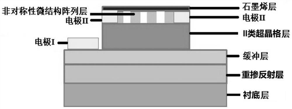
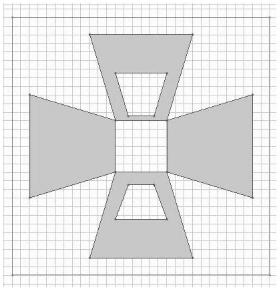
[0033] A type II superlattice infrared detector with a broadband absorption enhancement structure, comprising the following structure: a GaSb substrate layer with a thickness of 700 μm; a thickness of 1000 nm, the material is Be-doped GaSb, and the doping concentration is 1.5×10 19 / cm 3 The heavily doped reflective layer is epitaxially on the substrate layer; the GaSb buffer layer with a thickness of 1000 nm is epitaxially on the heavily doped reflective layer; the electrodes I and II superlattice layers are all arranged on the GaSb buffer layer; The symmetric microstructure array layer is arranged on the type II superlattice layer in the way that the electrode II surrounds the asymmetric microstructure array layer; the graphene layer with a thickness of 1 nm covers the electrode II and the asymmetric microstructure array layer; Among them, electrode I and electrode II are composed of 50nm Ti layer, 50nm Pt layer and 100nm Au layer stacked from bottom to top in sequence; the ...

Embodiment 2

[0041] A class II superlattice infrared detector with a broadband absorption enhancement structure, comprising the following structures: a GaSb substrate layer with a thickness of 800 μm; a thickness of 1500 nm, the material is Be-doped GaSb, and the doping concentration is 1×10 19 / cm 3 The heavily doped reflective layer is epitaxially on the substrate layer; the GaSb buffer layer with a thickness of 800 nm is epitaxially on the heavily doped reflective layer; the electrodes I and II superlattice layers are all arranged on the GaSb buffer layer; The symmetric microstructure array layer is arranged on the type II superlattice layer in the manner that the electrode II surrounds the asymmetric microstructure array layer; the graphene layer with a thickness of 0.5 nm covers the electrode II and the asymmetric microstructure array layer ; Among them, electrode I and electrode II are composed of 100nm Ti layer, 100nm Pt layer and 200nm Au layer stacked from bottom to top in sequenc...

Embodiment 3

[0049] A type II superlattice infrared detector with a broadband absorption enhancement structure, comprising the following structures: a GaSb substrate layer with a thickness of 500 μm; a thickness of 2000 nm, the material is Be-doped GaSb, and the doping concentration is 1.2×10 19 / cm 3 The heavily doped reflective layer is epitaxially on the substrate layer; the GaSb buffer layer with a thickness of 500 nm is epitaxially on the heavily doped reflective layer; the electrodes I and II superlattice layers are all arranged on the GaSb buffer layer; The symmetric microstructure array layer is arranged on the type II superlattice layer in the way that the electrode II surrounds the asymmetric microstructure array layer; the graphene layer with a thickness of 0.34 nm covers the electrode II and the asymmetric microstructure array layer ; Among them, electrode I and electrode II are composed of a Ti layer of 70 nm, a Pt layer of 70 nm and an Au layer of 150 nm from bottom to top. ...


PUM

PropertyMeasurementUnit
Thicknessaaaaaaaaaa
Thicknessaaaaaaaaaa
Doping concentrationaaaaaaaaaa

Abstract

The invention relates to a class-II superlattice infrared detector with a broadband absorption enhancement structure and a preparation method thereof, and belongs to the technical field of semiconductor infrared detectors. The detector comprises the following structures: a substrate layer; the heavily doped reflecting layer extends on the substrate layer; the buffer layer is epitaxially arranged on the heavily doped reflecting layer; the electrode I type superlattice layer and the electrode II type superlattice layer are arranged on the buffer layer; the electrode II and the asymmetric microstructure array layer are arranged on the type-II superlattice layer in a manner that the electrode II surrounds the asymmetric microstructure array layer; and the graphene layer covers the electrode II and the asymmetric microstructure array layer. An asymmetric plasma structure is constructed through a heavily doped reflecting layer, an intermediate class-II superlattice layer and an asymmetric microstructure array layer with a specific structure on the class-II superlattice layer, so that the light response speed, the specific detection rate and the absorptivity of the infrared detector are improved, and the dark current of the infrared detector is reduced. The detector has a broadband absorption enhancement function, is short in manufacturing period and low in cost, and is suitable for expanded production.

Description

technical field [0001] The invention belongs to the technical field of semiconductor infrared detectors, in particular to a class II superlattice infrared detector with a broadband absorption enhancement structure and a preparation method thereof. Background technique [0002] Infrared detectors are the core devices for perceiving and acquiring target infrared radiation information. They have the characteristics of high spatial identification, suitable for all-weather work and harsh environments, and have important application value in many fields of national major needs and national economic development. [0003] Type II superlattice material is a new type of infrared detection material that has developed rapidly at home and abroad in recent years. It has the characteristics of adjustable band gap, wide coverage detection wavelength, high theoretical detection rate, and strong compatibility with III-V semiconductor technology. , is the preferred material for the next genera...

Claims


Application Information

Patent Timeline
IPC IPC(8): H01L31/102H01L31/0216H01L31/0304H01L31/0352H01L31/18
CPCH01L31/035236H01L31/02168H01L31/03042H01L31/184H01L31/102Y02P70/50
Inventor 朱鹏孙泰史浩飞肖磊魏兴战熊稳
Owner CHONGQING INST OF GREEN & INTELLIGENT TECH CHINESE ACADEMY OF SCI
Why Eureka
Try Eureka