2D ga1- x in x se alloy and its preparation method and its application in the preparation of photoelectric detection
A photodetector and alloy technology, applied in selenium/tellurium compounds, chemical instruments and methods, circuits, etc., can solve the problems of low photodetection performance and small detection range, and achieve wide photoresponse range, good stability, good The effect of photodetection performance
- Summary
- Abstract
- Description
- Claims
- Application Information
AI Technical Summary
Problems solved by technology
Method used
Image
Examples
Embodiment 1 2
[0040] Example 1 Two-dimensional Ga 1-x In x Preparation of Se alloy
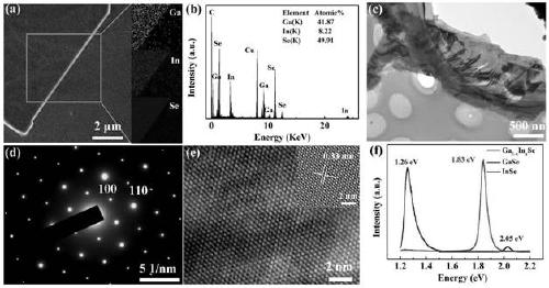
[0041] Step 1. Put 338mg of selenium powder and 300mg of indium-gallium eutectic alloy into the quartz boat, then put the quartz boat into the tube furnace and evacuate the tube furnace to 60Torr, and feed 20sccmAr, and keep the furnace temperature at 15 minutes Raise to 300°C and keep for 60 minutes; raise the temperature to 960°C in 33 minutes and keep for 120 minutes; cool down to room temperature in 19 minutes to prepare bulk Ga 1-x In x Se alloy material;
[0042] Step two, the 300nmSiO 2 Immerse the / Si substrate in a mixture of concentrated sulfuric acid-hydrogen peroxide (volume ratio: 3:1) at 83°C for 30 minutes, and then use isopropanol, acetone, ethanol, and ultrapure water for 10KHz ultrasonic treatment, and the ultrasonic treatment time is 10 minutes, blow dry with nitrogen, and set aside;
[0043] Step 3: Use Scotch single-sided transparent tape to repeatedly paste the block Ga 1-x In ...
Embodiment 2 2
[0044] Embodiment 2 two-dimensional Ga 1-x In x Fabrication of Se Alloy Electric Detectors
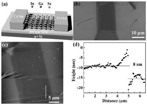
[0045] Select the 300nmSiO prepared in Example 1 2 2D Ga with a lateral dimension of 40 μm and a thickness of 8 nm on the surface of Si 1-x In x Se alloy, covered with two-dimensional Ga by fixing copper mask plate with silver glue 1-x In x The center position of the Se alloy, leaving two-dimensional Ga on both sides 1-x In x The Se alloy has a width of 3 μm, and then placed in a vacuum coating machine at a vacuum degree of 2×10 -4 Under the condition of Pa, in two-dimensional Ga 1-x In x On one side of the Se alloy, 5nm metal chromium and 40nm metal gold electrodes are sequentially evaporated to obtain a two-dimensional Ga 1-x In x Se alloy photodetector.
Embodiment 3 2
[0046] Embodiment 3 two-dimensional Ga 1-x In x Preparation of Se alloy
[0047] Step 1. Put 338mg of selenium powder and 300mg of indium-gallium eutectic alloy into the quartz boat, then put the quartz boat into the tube furnace and evacuate the tube furnace to 50Torr, and feed 30sccmAr, and keep the furnace temperature at 8 minutes Raise to 300°C and keep for 90 minutes; raise the temperature to 960°C for 20 minutes and keep for 140 minutes; cool down to room temperature for 15 minutes to prepare bulk Ga 1-x In x Se alloy material;
[0048] Step two, the 300nmSiO 2 Immerse the / Si substrate in a mixture of concentrated sulfuric acid-hydrogen peroxide (volume ratio: 3:1) at 83°C for 30 minutes, and then use isopropanol, acetone, ethanol, and ultrapure water for 20KHz ultrasonic treatment, and the ultrasonic treatment time is 15 minutes, blow dry with nitrogen, and set aside;
[0049] Step 3: Use Scotch single-sided transparent tape to repeatedly paste the block Ga 1-x ...
PUM
| Property | Measurement | Unit |
|---|---|---|
| thickness | aaaaa | aaaaa |
| size | aaaaa | aaaaa |
| thickness | aaaaa | aaaaa |
Abstract
Description
Claims
Application Information


