

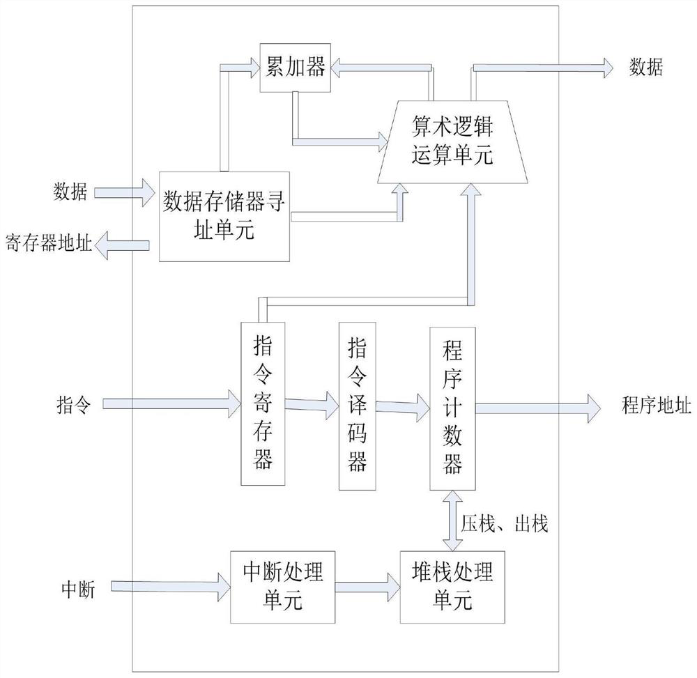
An 8-bit risc-cpu system
A RISC-CPU, n-1 technology, applied in the field of 8-bit RISC-CPU system, can solve the problems of inflexible addressing mode, reduced code efficiency and addressing efficiency, and achieve efficient addressing and improve code efficiency.
- Summary
- Abstract
- Description
- Claims
- Application Information
AI Technical Summary
Problems solved by technology
Method used
Image

Examples
Embodiment 1
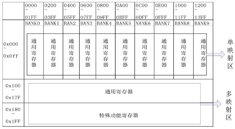
[0047]Embodiment one: this implementation is a data register address mapping method of an 8-bit RISC-CPU system: the method divides the logical address into a single mapping area and a multi-mapping area, and a logical address in a single mapping area corresponds to an actual physical address, and Divided into different banks, one actual physical address in the multi-mapping area has multiple logical addresses, the single-mapping area is all general-purpose registers, and the multi-mapping area has general-purpose registers and special function registers.
[0048] The principle of mapping partitions and sub-banks is as follows:
[0049] Divide the logical address into low 8 bits and high n bits, where n is less than 8, which is determined by the total size of the data memory composed of the RAM connected to the CPU (as a general-purpose register) and special function registers. The size of the data memory is 5k, that is, the maximum code Take the address 0x13FF as an example, ...
Embodiment 2
[0052] Embodiment two: as attached figure 2 Shown, the data memory structure of the present invention, this figure is 0x13FF with the maximum logic address of data memory, and the general-purpose register and the special function register of the multi-mapping area each account for half as an example, first according to "the logic address whose address high n bits are an even number The area is a single-mapping area, and the logical address area with an odd number is multi-mapping area” method to partition the address, the logical address of the single-mapping area (hexadecimal): 0000~00FF (BANK0), 0200~02FF (BANK1), 0400~04FF (BANK2), 0600~06FF(BANK3), 0800~08FF(BANK4), 0A00~0AFF(BANK5), 0C00~0CFF(BANK6), 0E00~0EFF(BANK7), 1000~10FF(BANK8), 1200~12FF( BANK9), this area is generally used as a general-purpose register, and each logical address corresponds to an actual physical address of RAM; the logical address of the multi-mapping area (hexadecimal): 0100~01FF, 0300~03FF, 050...
Embodiment 3
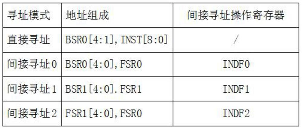
[0053] Embodiment three: as attached image 3 As shown, the address composition modes of the 4 kinds of addressing modes of the data memory of the present invention and the related indirect addressing operation registers, a few specific examples are given below, combined with the attached figure 2 To illustrate the addressing operation of the present invention:
[0054] Direct addressing:
[0055]
[0056]
[0057] The above program realizes 3 operations: lines 2 and 3 pass the value of 0x210 to 0x110; lines 4 and 5 pass the value of 0x211 to 0x180; lines 6 and 7 pass the value of 0x180 to 0x212.
[0058] Among them, 0x210, 0x211, and 0x212 are general-purpose registers in the single-mapping area, 0x110 are general-purpose registers in the multi-mapping area, and 0x180 and 181 are special function registers in the multi-mapping area.
[0059] The above transmission process only needs to use the page cutting instruction BANKBSR0 to write the high address of 0x210 into ...
PUM
 Abstract
Description
Claims
Application Information