Bipolar transistor with polysilicon emitter and method of manufacturing
A semiconductor and assembly technology, which is applied in the manufacture of semiconductor/solid-state devices, semiconductor devices, electrical components, etc., and can solve problems such as increasing the resistance of the collector area.
- Summary
- Abstract
- Description
- Claims
- Application Information
AI Technical Summary
Problems solved by technology
Method used
Image

Examples
Embodiment Construction
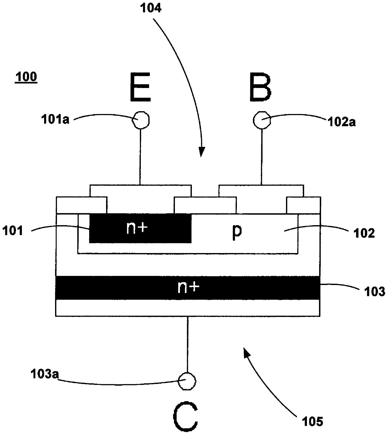
[0030] will now refer to Figures 2a to 2l , by way of example only, a step-by-step description of a fabrication process of a bipolar transistor according to one or more embodiments is provided. In this example, the bipolar device is an NPN device. An equivalent PNP device can be realized by simply exchanging dopant N and dopant P.
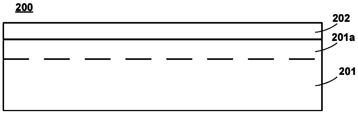
[0031] Figure 2a A starting substrate 201 for manufacturing a semiconductor device according to an embodiment is shown. At this stage, a collector epitaxial layer 201 a is deposited on the top surface of the substrate 201 , so that the semiconductor device may include a low doped N collector epitaxial layer deposited on a highly doped N substrate 201 . For substrate resistivities in the range of about 1 mΩcm to 10 mΩcm, the N doping in the substrate 201 is substantially higher, for example 10000 times, than the N doping in the collector epitaxial layer. In this example, the substrate 201 needs to be highly doped to achieve a low saturation vo...
PUM
 Abstract
Description
Claims
Application Information
 - R&D
- Intellectual Property
- Life Sciences
- Materials
- Tech Scout
- Unparalleled Data Quality
- Higher Quality Content
- 60% Fewer Hallucinations
Browse by: Latest US Patents, China's latest patents, Technical Efficacy Thesaurus, Application Domain, Technology Topic, Popular Technical Reports.
© 2025 PatSnap. All rights reserved.Legal|Privacy policy|Modern Slavery Act Transparency Statement|Sitemap|About US| Contact US: help@patsnap.com