Electromagnetic wave absorbing film and electromagnetic wave absorbing composite substrate including same
An electromagnetic wave, absorbing film technology, applied in the reduction of crosstalk/noise/electromagnetic interference (circuit devices, electrical components, etc., can solve problems such as thickening thickness, difficult to cope with the trend of thinning terminal equipment, etc., to simplify the manufacturing process. , to ensure the effect of magnetic permeability and high magnetic permeability
- Summary
- Abstract
- Description
- Claims
- Application Information
AI Technical Summary
Problems solved by technology
Method used
Image
Examples
Embodiment 1~6
[0116] 1-1. Production of thermosetting composition for electromagnetic wave absorbing layer formation
[0117] The components of the thermosetting composition for forming an electromagnetic wave absorbing layer were mixed and manufactured according to the ratio of the compounding example of the following [Table 1]. The usage unit of each composition in the following Table 1 is parts by weight.
[0118] 1-2. Manufacture of electromagnetic wave absorbing film
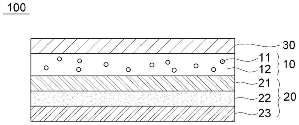
[0119] On one side of the polyimide layer (12 μm), apply the thermosetting composition for forming an electromagnetic wave absorbing layer in the above 1-1 to form an electromagnetic wave absorbing layer (PMS layer), and make it dry to a thickness of 60 μm. The adhesive layer (12 μm) was sequentially applied and dried, and a release paper was arranged to produce a cover film layer with a thickness of 24 μm.
[0120] After arranging a protective film composed of a polyimide layer (25-50 μm) with an adhesive layer (P...
experiment example 1
[0134] The properties of the electromagnetic wave absorbing films produced in Examples 1 to 6 and Comparative Examples 1 to 2 were measured according to the following measurement methods, and the results are shown in Table 1 above.
[0135] 1) Peel strength
[0136] According to JIS C6471, when the electromagnetic wave absorbing layer (PMS layer) is peeled at a speed of 50 mm / min at a rate of 50 mm / min under the condition of 25 ° C, the surface of the polyimide (PI) layer of the above-mentioned cover film is measured at 90 degrees. The minimum force required and expressed as peel strength.
[0137] 2) Evaluation of heat resistance
[0138] According to JIS C6471, the electromagnetic wave absorbing film was cut|disconnected by 25 mm square, the test piece was manufactured, and this test piece was floated on the solder bath of 288 degreeC. Then, the time until blisters occurred on the surface of the electromagnetic wave absorbing film was measured.
[0139] 3) Permeability ev...
PUM
| Property | Measurement | Unit |
|---|---|---|
| peel strength | aaaaa | aaaaa |
| peel strength | aaaaa | aaaaa |
| thickness | aaaaa | aaaaa |
Abstract
Description
Claims
Application Information
 - R&D
- Intellectual Property
- Life Sciences
- Materials
- Tech Scout
- Unparalleled Data Quality
- Higher Quality Content
- 60% Fewer Hallucinations
Browse by: Latest US Patents, China's latest patents, Technical Efficacy Thesaurus, Application Domain, Technology Topic, Popular Technical Reports.
© 2025 PatSnap. All rights reserved.Legal|Privacy policy|Modern Slavery Act Transparency Statement|Sitemap|About US| Contact US: help@patsnap.com


