Diode production and manufacturing process

A manufacturing process and diode technology, applied in semiconductor/solid-state device manufacturing, electrical components, circuits, etc., can solve the problems of incomplete sealing, poor mold clamping effect, diode surface defects, etc., to ensure the use effect and reduce glue waste. , to avoid flawed effects

Inactive Publication Date: 2020-06-26
丁晟
View PDF0 Cites 0 Cited by
  • Summary
  • Abstract
  • Description
  • Claims
  • Application Information

AI Technical Summary

Problems solved by technology

[0005] The present invention can solve the problem that when the existing equipment molds the black glue layer outside the diode, usually the black glue is stuffed into the molding machine, and then molded by heating and softening, resulting in poor processing effect and low efficiency of the diode. The processing cost of the diode is increased, and when the existing equipment is used for molding the diode, the mold clamping effect is poor, the sealing is not complete, and the phenomenon of glue leakage is prone to occur, resulting in defects on the surface of the processed diode, which affects the use effect of the diode, etc. problem

Method used


Image

  • Diode production and manufacturing process
  • Diode production and manufacturing process
  • Diode production and manufacturing process

Examples


Embodiment Construction

[0035] The embodiments of the present invention will be described in detail below with reference to the accompanying drawings, but the present invention can be implemented in many different ways defined and covered by the claims.

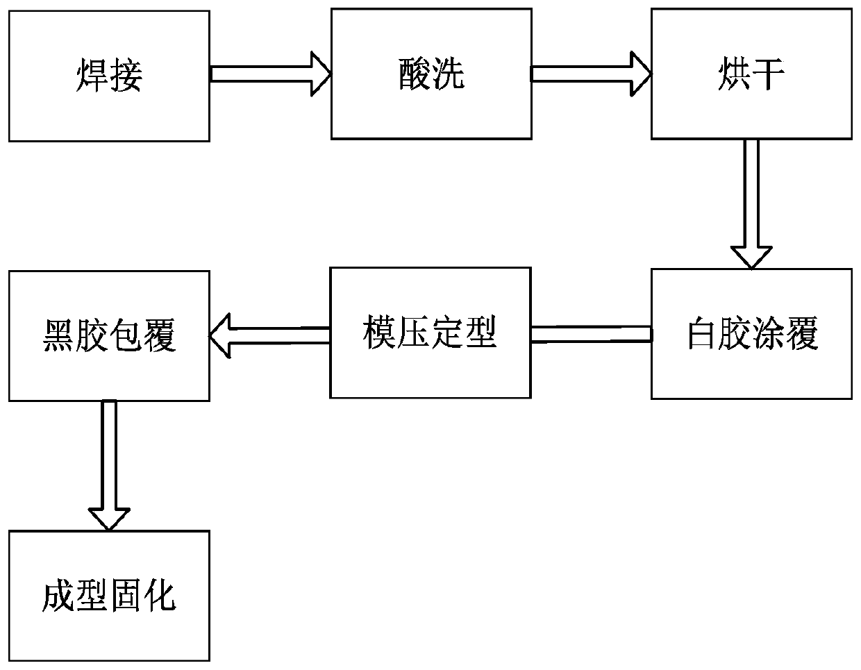
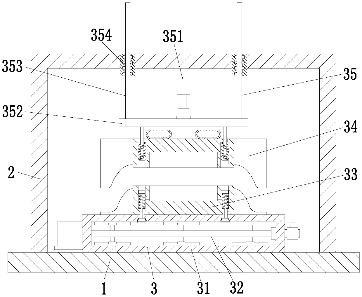
[0036] like Figure 1 to Figure 5 As shown, a diode production and manufacturing process, the diode production and manufacturing process adopts the following processing equipment, the processing equipment includes a base plate 1, a support frame 2 and a molding device 3, the upper end of the base plate 1 is equipped with a support frame 2, a support frame 2 The cross-section is U-shaped, and the cross-section of the support frame 2 is U-shaped. A molding device 3 is arranged inside the support frame 2 , and the lower end of the molding device 3 is installed in the middle of the upper end of the bottom plate 1 .

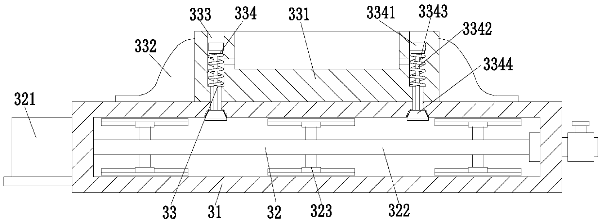
[0037]The molding device 3 includes a housing frame 31, a stirring mechanism 32, a lower mold frame 33, an upper mold frame 34, and a mold...


PUM


Abstract

The invention relates to a diode production and manufacturing process, which comprises a bottom plate, a support frame and a mold pressing device. The support frame is arranged at the upper end of thebottom plate, the section of the support frame is of a U-shaped structure, the mold pressing device is arranged in the support frame, and the lower end of the mold pressing device is arranged in themiddle of the upper end of the bottom plate. By using the diode production and manufacturing process, the problems as follows can be solved: when a black adhesive layer on the outer side of a diode issubjected to a mold pressing process by means of existing equipment, generally, black adhesive is stuffed into a molding press, and mold pressing is carried out through heating and softening, which leads to the problems of poor diode processing effect, low efficiency, and increase in diode processing cost; and moreover, when mold pressing is carried out on a diode by the existing equipment, the mold closing effect is poor, sealing is incomplete, adhesive leakage occurs easily, there are defects on the surface of the processed diode, the use effect of the diode is affected.

Description

technical field [0001] The invention relates to the field of diode production and manufacturing, in particular to a diode production and manufacturing process. Background technique [0002] Diode is one of the earliest semiconductor devices, and its application is very wide. Especially in various electronic circuits, use diodes and resistors, capacitors, inductors and other components to make reasonable connections to form circuits with different functions, which can realize AC rectification, modulation signal detection, amplitude limiting and clamping, and power supply Voltage regulation and other functions. [0003] At present, the existing diodes usually have the following defects in the production and manufacturing process: 1. When the existing equipment molds the black glue layer outside the diode, it usually inserts the black glue into the molding machine, and then softens it by heating Molding processing leads to poor processing effect and low efficiency of the diod...

Claims


Application Information

Patent Timeline
Patent Type & Authority Applications(China)
IPC IPC(8): H01L21/50H01L21/56H01L21/329
CPCH01L21/50H01L21/56H01L21/565H01L29/6609
Inventor 丁晟韦名典
Owner 丁晟
Why Eureka
Try Eureka