Organic electro-luminescent display apparatus

Inactive Publication Date: 2009-06-11
HITACHI LTD
View PDF4 Cites 35 Cited by
  • Summary
  • Abstract
  • Description
  • Claims
  • Application Information

AI Technical Summary

Benefits of technology

[0022]According to the present invention, it becomes possible to provide the organic electro-luminescent display apparatus which is capable of implementing the compatibility between the stagger-type polycrystalline-Si TFT structure having excellent characteristics and the low-resistance line structure advantageous for the large-sized implementation of the display, which is advantageous from the cost-based viewpoint as well as the performance-based viewpoint. Also, the wiring lines disposed at the upper layer as compared with

Problems solved by technology

The necessary processing-step number, however, increases as the structure becomes complicated.
Accordingly, the fabrication becomes significantly disadvantageous from the cost-based viewpoint.
For the practical implementation of the stagger-type polycrystalline-Si TFT structure, however, there exist the following problems to be solved.
Consequently, heat damage to the electrodes and lines has been unavoidable.
Consequently, there have existed limits to the line material and the structure, e.g., a high-melting-point metallic material must be used instead of the usually-

Method used


Image

  • Organic electro-luminescent display apparatus
  • Organic electro-luminescent display apparatus
  • Organic electro-luminescent display apparatus

Examples


Example

EMBODIMENT 1

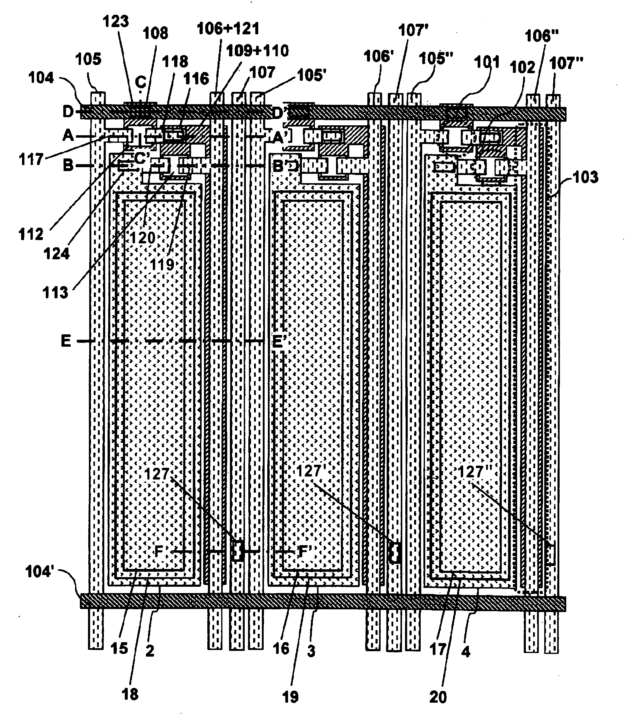
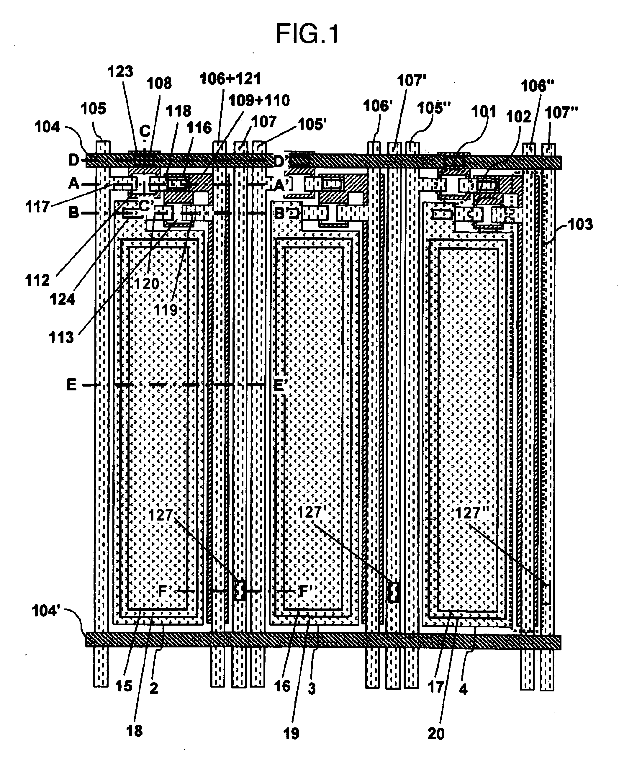
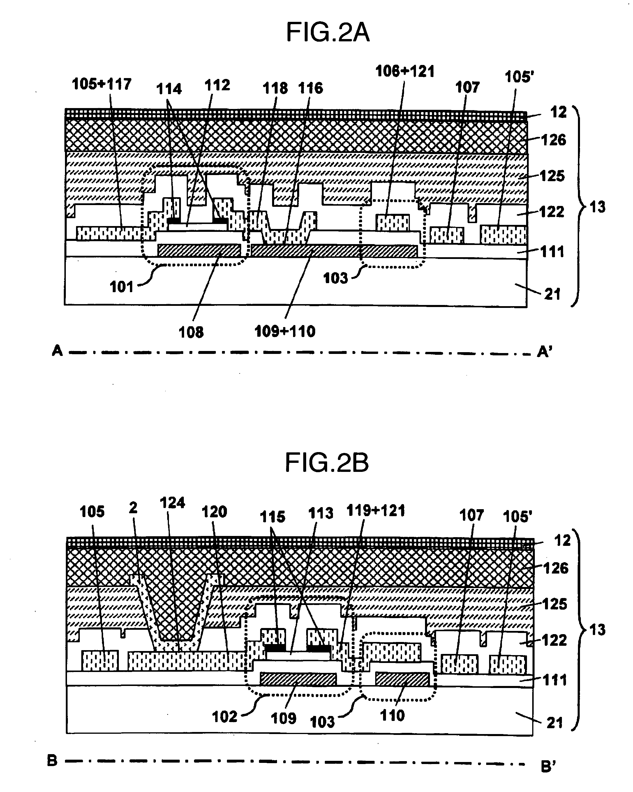
[0097]FIG. 1 is a plane view of one color pixel of an organic electro-luminescent display apparatus according to a first embodiment of the present invention. Here, one color pixel was configured with three-primary-color subpixels of green, red, and blue. Also, FIG. 2A is a cross-sectional view of the apparatus along an A-A′ line in FIG. 1. FIG. 2B is a cross-sectional view of the apparatus along a B-B′ line in FIG. 1 similarly. FIG. 2C is a cross-sectional view of the apparatus along a C-C′ line in FIG. 1 similarly. FIG. 2D is a cross-sectional view of the apparatus along a D-D′ line in FIG. 1 similarly. FIG. 2E is a cross-sectional view of the apparatus along an E-E′ line in FIG. 1 similarly. FIG. 2F is a cross-sectional view of the apparatus along an F-F′ line in FIG. 1 similarly.

[0098]In FIG. 1 and FIG. 2A to FIG. 2F, on a glass substrate 21, a plurality of scanning lines 104 were arranged with a constant spacing placed therebetween. Simultaneously, a plurality of sig...

Example

[0131]Also, in the above-described first embodiment, as illustrated in FIG. 2I and FIG. 2J, it is of curse possible to form the bottom-emission-type organic electro-luminescent display apparatus which extracts light from the side of the lower electrode 2. This is made possible by configuring the lower electrode 2 of each organic electro-luminescent element with a transparent electrically-conductive oxide film such as ITO, and by configuring the upper transparent electrode 12 with a metal having excellent refection property such as Al. As described earlier, the ITO and Al films can be formed by using the sputtering method or vacuum evaporation method.

[0132]Also, in the above-described first embodiment, the configuration has been employed where the entire surface of the first transistor 101 and the second transistor 102 was coated with the second interlayer insulation film 125 which serves as the planarization film as well. On account of this configuration, when forming the top-emissi...

Example

EMBODIMENT 2

[0133]FIG. 5 is a plane view of one color pixel of an organic electro-luminescent display apparatus according to a second embodiment of the present invention. FIG. 6A is a cross-sectional view of the apparatus along an A-A′ line. FIG. 6B is a cross-sectional view of the apparatus along a B-B′ line. FIG. 6C is a cross-sectional view of the apparatus along a C-C′ line. FIG. 6D is a cross-sectional view of the apparatus along a D-D′ line. FIG. 6E is a cross-sectional view of the apparatus along an E-E′ line. FIG. 6F is a cross-sectional view of the apparatus along an F-F′ line. The point which differs from the above-described first embodiment is as follows: The gate line 104 of the present invention disposed at the upper layer as compared with the semiconductor layers 112 and 113, and the auxiliary line 107 of the upper transparent electrode 12, i.e., the second current supply line 107, were configured with the same layer and the same component. Based on this feature, while...


PUM


Abstract

Each TFT for driving each of a plurality of pixels arranged in a matrix-like configuration is configured using a stagger-type polycrystalline-Si TFT. A gate electrode, which is composed of a high-heat-resistant material capable of resisting high temperature at the time of polycrystalline-Si film formation, is disposed at a lower layer as compared with the polycrystalline-Si layer that forms a channel of each TFT. A gate line, which is composed of a low-resistance material, is disposed at an upper layer as compared with the polycrystalline-Si layer. The gate electrode and the gate line are connected to each other via a through-hole bored in a gate insulation film. Respective configuration components of each organic electro-luminescent element are partially co-used at the time of the line formation, thereby suppressing an increase in the steps, processes, and configuration components.

Description

BACKGROUND OF THE INVENTION[0001]1. Field of the Invention[0002]The present invention relates to an organic electro-luminescent display apparatus. More particularly, it is preferable for an organic electro-luminescent display apparatus provided with a polycrystalline-Si TFT structure having excellent characteristics.[0003]2. Description of the Related Art[0004]In accompaniment with the arrival of full-fledged multimedia age, attention has been focused on organic electro-luminescent display apparatus as a next-generation flat-plane-type display apparatus which are expected to replace the conventional liquid-crystal display apparatus. The organic electro-luminescent display apparatus exhibits excellent characteristics such as spontaneous light, wide field-of-view angle, and high-speed response characteristics. In the so-called bottom-emission-type organic electro-luminescent display apparatus, which is one type of the organic electro-luminescent display apparatuses, a large number of ...

Claims


Application Information

Patent Timeline
IPC IPC(8): G09G3/30
CPCH01L27/3262H01L2227/323H01L27/3276H10K59/1213H10K59/131H10K59/1201
Inventor NISHIMURA, ETSUKOWAKAGI, MASATOSHIONISAWA, KENICHIMATSUMURA, MIEKO
Owner HITACHI LTD
Why Eureka
Try Eureka