Method of cutting semiconductor wafer and protective sheet used in the cutting method

a technology of protective sheets and semiconductor wafers, which is applied in the direction of semiconductor devices, semiconductor/solid-state device details, electrical devices, etc., can solve the problems of reducing the yield of machining, reducing the strength of semiconductor elements, and reducing the thickness of semiconductor elements, so as to prevent the fluctuation of plasma etching progress and suppress the progress of plasma etching

Inactive Publication Date: 2006-06-13
PANASONIC CORP
View PDF7 Cites 60 Cited by
  • Summary
  • Abstract
  • Description
  • Claims
  • Application Information

AI Technical Summary

Benefits of technology

[0008]Therefore, it is an object of the present invention to provide a method of cutting a semiconductor wafer capable of preventing a protective sheet from being damaged by heat when the semiconductor wafer is cut by plasma etching. It is also an object of the present invention to provide the protective sheet used in the method of cutting the semiconductor wafer.
[0014]According to the present invention, in a method of cutting a semiconductor wafer by plasma etching, a protective sheet is used, on which a metallic layer, a plasma etching rate of which is lower than that the semiconductor wafer, is formed on one face of an insulating sheet which is the base material, and this metallic layer is utilized as an etching stop layer for suppressing the progress of plasma etching. Due to the foregoing, it is possible to realize operation of effective plasma etching in which fluctuation of the progress of plasma etching is avoided, so that the occurrence of heat damage given to a protective sheet in the process of cutting can be prevented.

Problems solved by technology

The mechanical strength of the semiconductor element, the thickness of which is reduced, is so low that the semiconductor element is liable to break in the process of cutting conducted in the dicing step in which the semiconductor element in the state of a wafer is cut into individual pieces, and the yield of machining is inevitably lowered.
However, in the process of plasma dicing of the prior art described above, due to the want of uniformity of etching action conducted by plasma, the following problems are caused and have not been solved yet.
In this connection, an etching rate showing the degree of etching conducted by plasma is not necessarily uniform.
As a result, there is a possibility that the protective sheet is superheated, burned and deformed.
According to the conventional plasma dicing method, it is impossible to effectively prevent the protective sheet from being damaged by heat caused by the want of uniformity of the etching action of plasma.

Method used


Image

  • Method of cutting semiconductor wafer and protective sheet used in the cutting method
  • Method of cutting semiconductor wafer and protective sheet used in the cutting method
  • Method of cutting semiconductor wafer and protective sheet used in the cutting method

Examples


Embodiment Construction

[0021]Next, referring to the drawings, an embodiment of the present invention will be explained below.

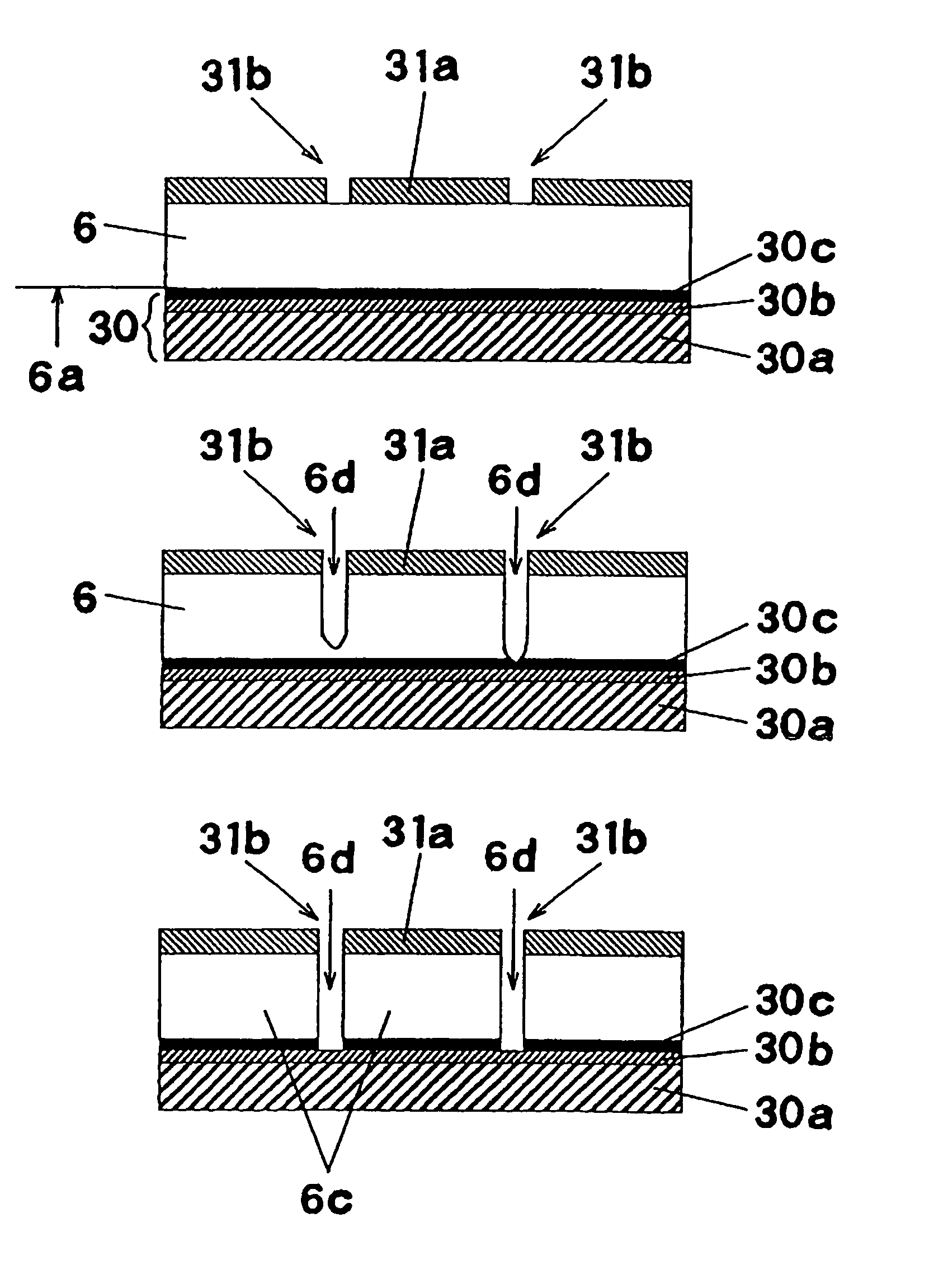
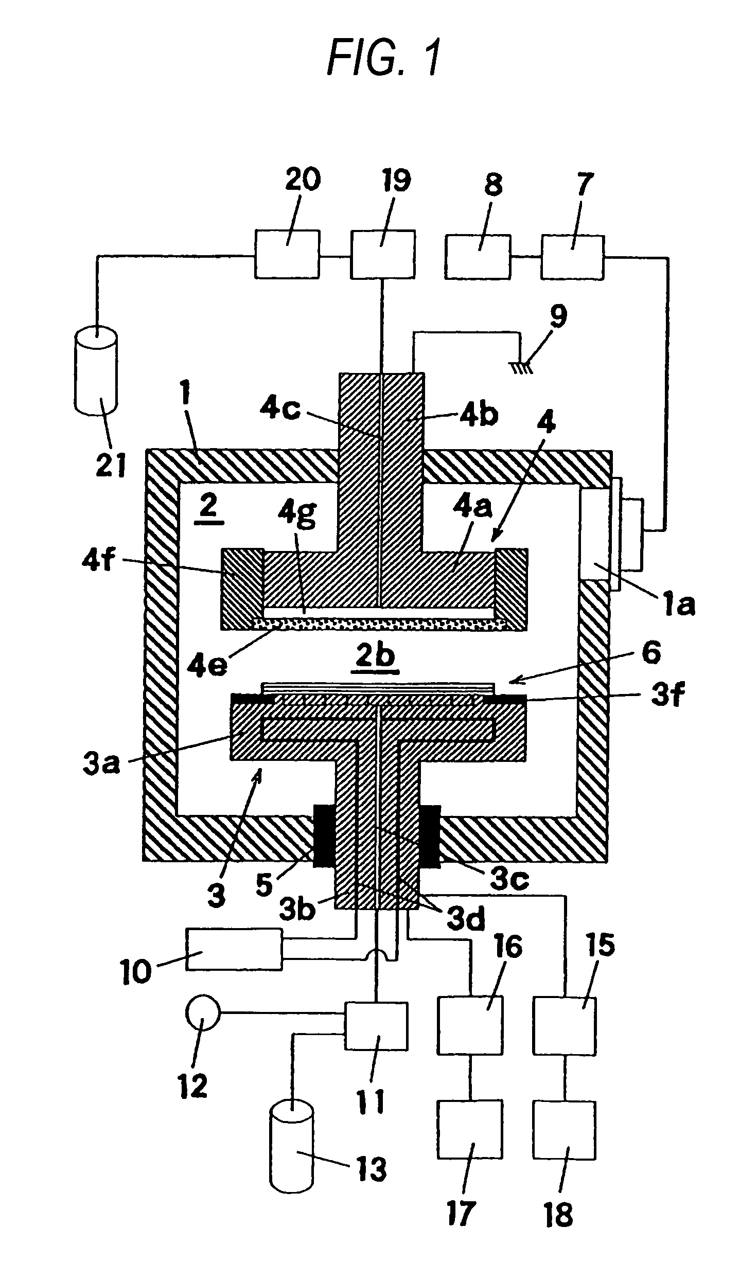
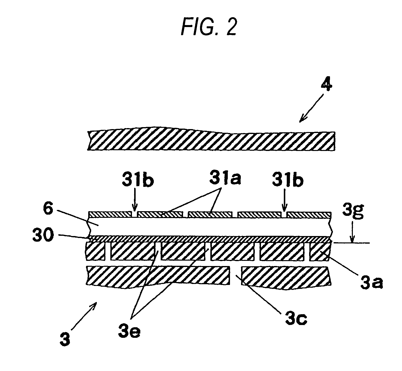
[0022]First, referring to FIGS. 1 to 3(b), the plasma processing device will be explained below. This plasma processing device is used in the manufacturing process of a semiconductor device obtained in such a manner that a semiconductor wafer, on the circuit forming face (the first face) of which a plurality of semiconductor elements are formed, is divided into individual piece of the semiconductor elements so as to obtain a semiconductor device, the thickness of which is not more than 100 μm.

[0023]In the manufacturing process of this semiconductor device, first of all, a protective sheet made of material, a plasma etching rate of which is lower compared with silicon that is a primary material of the semiconductor, is attached to the circuit forming face of the semiconductor wafer. On the reverse face opposite to the circuit forming face of the semiconductor wafer, a mask to determi...


PUM

PropertyMeasurementUnit
thicknessaaaaaaaaaa
metallicaaaaaaaaaa
sizeaaaaaaaaaa

Abstract

In a method of cutting a semiconductor wafer in which the semiconductor wafer 6 is cut by plasma etching, a protective sheet 30 on which a metallic layer 30b, a plasma etching rate of which is low, is formed on one face of an insulating sheet 30a is stuck on to a circuit forming face 6a by an adhesive layer 30c, and plasma is exposed onto an opposite side to the circuit forming face 6a from a mask side which is formed by covering regions except for cutting lines 31b with a resist film 31a so as to conduct plasma etching on portions of the cutting lines. Due to the above structure, it is possible to use the metallic layer as an etching stop layer for suppressing the progress of etching. Therefore, fluctuation of the progress of etching can be avoided and heat damage caused on the protective sheet can be prevented.

Description

BACKGROUND OF THE INVENTION[0001]The present invention relates to a method of cutting a semiconductor wafer by means of plasma etching. The present invention also relates to a protective sheet used in the method of cutting the semiconductor wafer.[0002]A semiconductor device mounted on a board of electronic equipment is conventionally manufactured in such a manner that pins of a lead frame and metallic bumps are connected to semiconductor elements, on which a circuit pattern is formed in the state of a wafer, and the semiconductor elements are subjected to a packaging process so that they can be sealed with resin. Since the size of electronic equipment has been recently reduced, the size of the semiconductor device has been also decreased. Especially, investigations are actively made into the reduction of the thickness of a semiconductor element.[0003]The mechanical strength of the semiconductor element, the thickness of which is reduced, is so low that the semiconductor element is ...

Claims


Application Information

Patent Timeline
Patent Type & Authority Patents(United States)
IPC IPC(8): H01L21/50H01L21/3065C09J7/02H01L21/301H01L21/302H01L21/46H01L21/461H01L21/68H01L21/78H01L23/52
CPCH01L21/6835H01L21/78H01L2221/6834H01L2924/0002H01L2924/00H01L21/3065
Inventor ARITA, KIYOSHI
Owner PANASONIC CORP
Why Eureka
Try Eureka