Semiconductor integrated circuit

a technology of integrated circuits and semiconductors, applied in the direction of semiconductor devices, diodes, electrical apparatus, etc., can solve the problems of increasing process cost, difficult for circuit designers to construct above-mentioned semiconductor integrated circuits, and difficult to integrate and construct semiconductor structures of different sizes on the same substrate, etc., to achieve the effect of increasing process cost and superior flexibility

Active Publication Date: 2014-11-06
UNITED MICROELECTRONICS CORP
View PDF8 Cites 35 Cited by
  • Summary
  • Abstract
  • Description
  • Claims
  • Application Information

AI Technical Summary

Benefits of technology

[0010]According to the semiconductor integrated circuit provided by the present invention, the multi-gate transistor device having the fin structures is integrated with the n-well resistor and / or the LDMOS device, which complies with high voltage requirement. Those different devices are electrically isolated by the first isolation structures and the second isolation structures of which the sizes are different. In other words, the semiconductor integrated circuit provided by the present invention renders superior flexibility to those circuit designers. In other words, the semiconductor integrated circuit having devices of different sized can be integrated without increasing process cost due to the flexibility rendered by the semiconductor integrated circuit of the present invention.

Problems solved by technology

However, the FinFET device still faces many problems.
For example, semiconductor structures of different sizes and isolation structures of different sizes are often formed on one semiconductor integrated circuit, and it is always difficult to construct and integrate those semiconductor structures and the isolation structures of different sizes on the same substrate.
Furthermore, it is difficult for the circuit designer to construct above mentioned semiconductor integrated circuit without increasing process cost.

Method used


Image

  • Semiconductor integrated circuit
  • Semiconductor integrated circuit
  • Semiconductor integrated circuit

Examples


Embodiment Construction

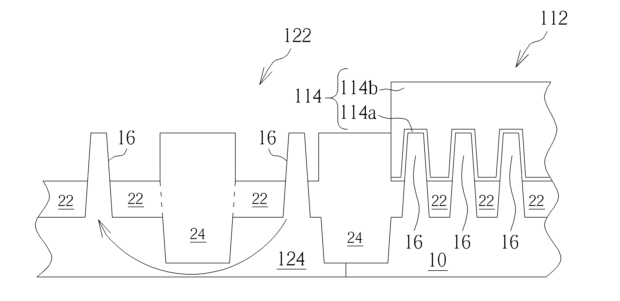
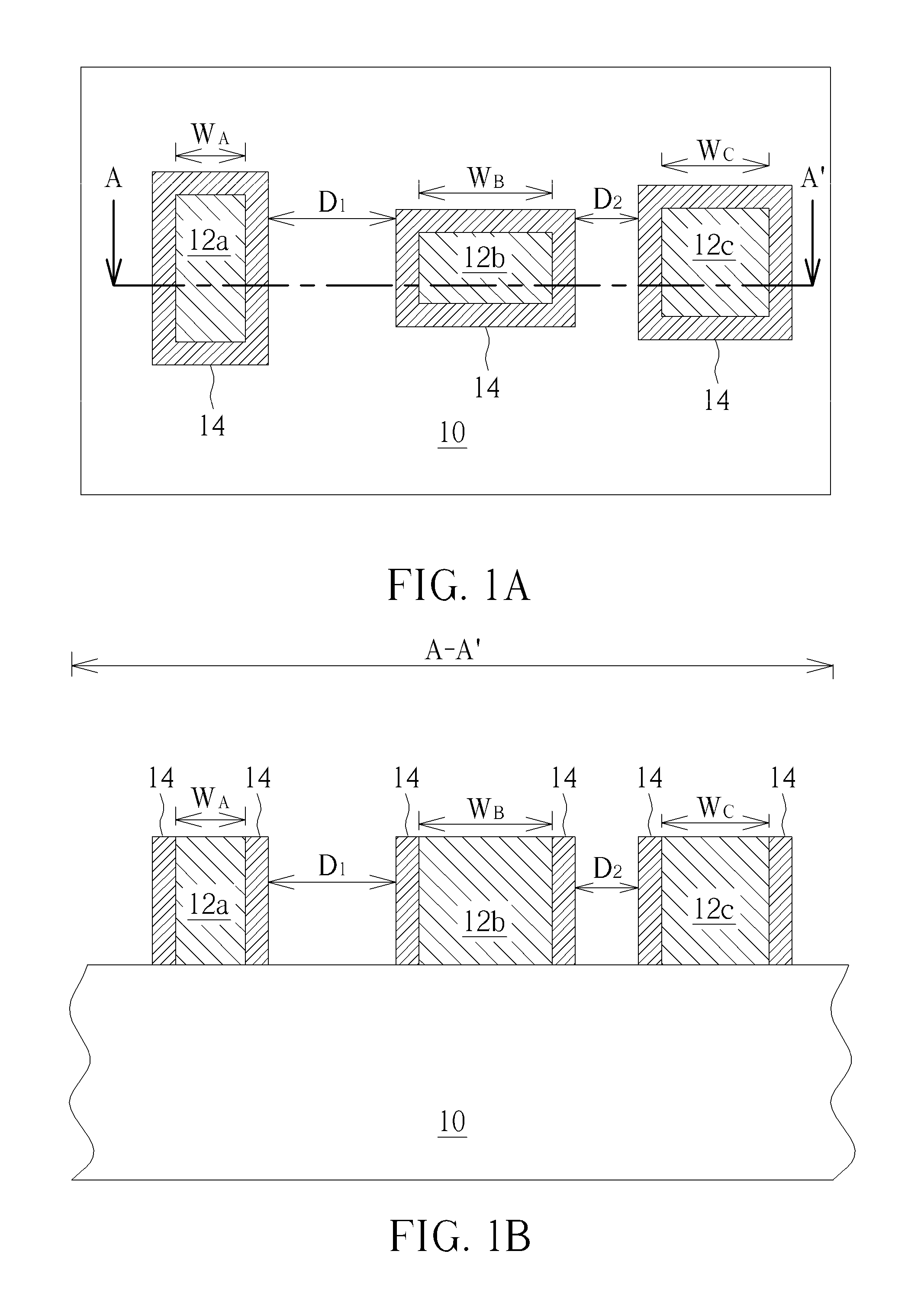
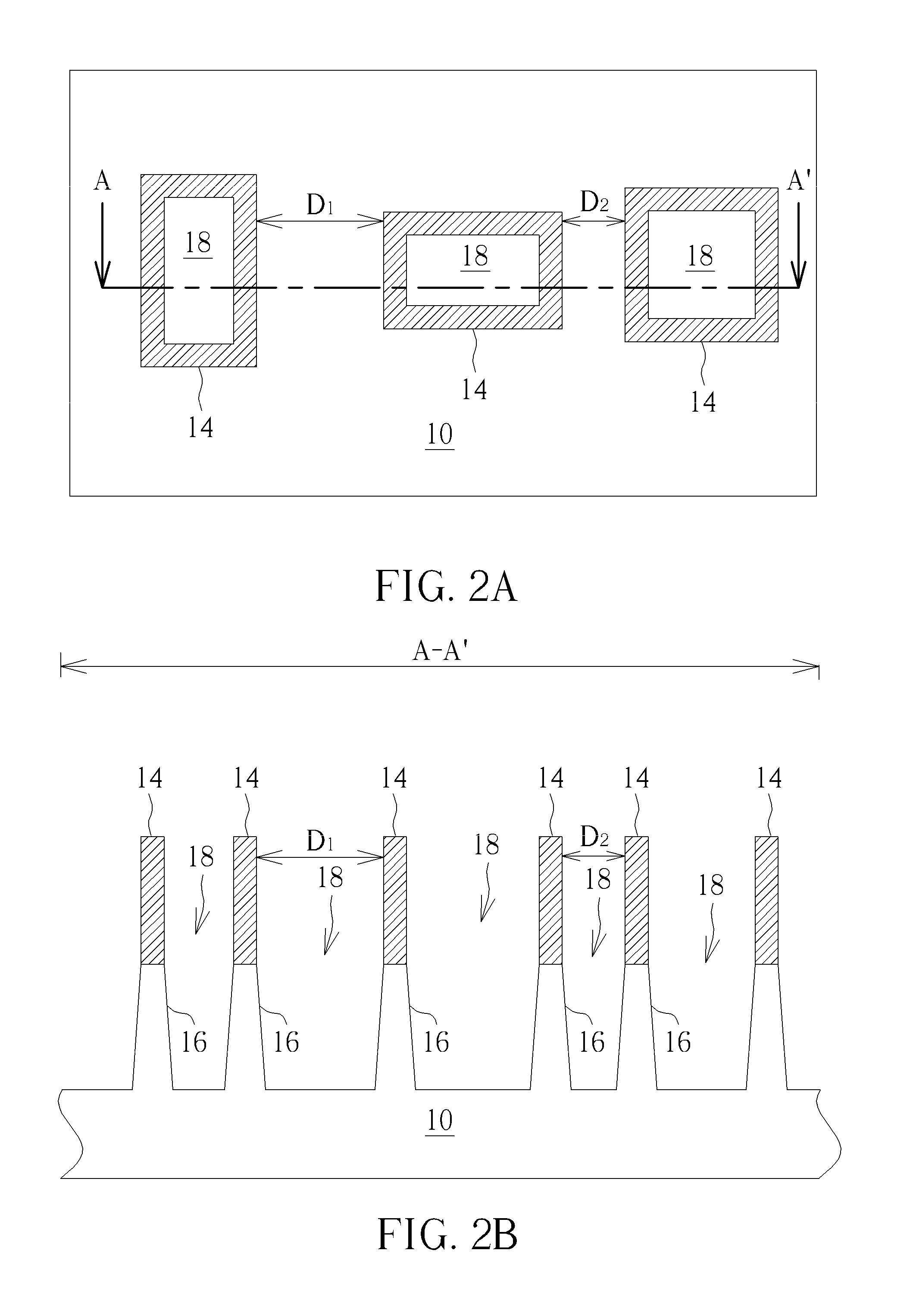
[0020]Please refer to FIGS. 1A-3B, which are schematic drawings illustrating a method for manufacturing isolation structures provided by a preferred embodiment of the present invention. FIGS. 1B, 2B, and 3B respectively are cross-sectional view taken along Line A-A′ of FIGS. 1A, 2A, and 3A. It is noteworthy that the method for manufacturing isolation structures provided by the preferred embodiment adopts an approach for manufacturing fin structures for multi-gate transistor device, namely, the spacer image transfer (SIT) approach. Therefore the isolation structures can be integrated with the fin structures for multi-gate transistor device according to the preferred embodiment. As shown in FIG. 1A and FIG. 1B, a substrate 10 is provided. The substrate 10 includes at least a silicon material layer. A pad layer (not shown) can be formed on a surface of the substrate 10 if required, and the pad layer can include oxides, nitride, or any other suitable materials. Next, a mandrel layer 12a...


PUM


Abstract

A semiconductor integrated circuit includes a substrate, a multi-gate transistor device formed on the substrate, and an n-well resistor formed in the substrate. The substrate includes a plurality of first isolation structures and at least a second isolation structure formed therein. A depth of the first isolation structures is smaller than a depth of the second isolation structure. The multi-gate transistor device includes a plurality of fin structures, and the fin structures are parallel with each other and spaced apart from each other by the first isolation structures. The n-well resistor includes at least one first isolation structure. The n-well resistor and the multi-gate transistor device are electrically isolated from each other by the second isolation structure.

Description

BACKGROUND OF THE INVENTION[0001]1. Field of the Invention[0002]The present invention relates to a semiconductor integrated circuit, and more particularly, to a semiconductor integrated circuit having multi-gate transistor device integrated with other devices such as resistor and / or lateral double-diffused metal-oxide-semiconductor (hereinafter abbreviated as LDMOS) device.[0003]2. Description of the Prior Art[0004]Conventional planar metal-oxide-semiconductor (hereinafter abbreviated as MOS) transistor has difficulty when scaling down to 65 nm and below. Therefore the non-planar transistor technology such as Fin Field effect transistor (FinFET) technology that allows smaller size and higher performance is developed to replace the planar MOS transistor.[0005]Since the manufacturing processes of the FinFET device are easily integrated into the traditional logic device processes, it provides superior process compatibility. More important, since the FinFET device increases the overlapp...

Claims


Application Information

Patent Timeline
Patent Type & Authority Applications(United States)
IPC IPC(8): H01L27/088H01L27/06
CPCH01L27/0629H01L27/0886H01L21/823431H01L27/0611H01L28/20H01L29/0649H01L29/0653H01L29/408H01L29/7816H01L29/7817H01L29/7835H01L29/7851
Inventor TSAO, PO-CHAO
Owner UNITED MICROELECTRONICS CORP
Why Eureka
Try Eureka