Semiconductor processing equipment

A technology for processing equipment and semiconductors, which is applied in the fields of semiconductor/solid-state device manufacturing, combined devices, electrical components, etc., and can solve problems affecting semiconductor wafer manufacturing processes and the overall yield decline of equipment.

Pending Publication Date: 2020-06-30
XIA TAI XIN SEMICON QING DAO LTD
View PDF0 Cites 2 Cited by
  • Summary
  • Abstract
  • Description
  • Claims
  • Application Information

AI Technical Summary

Problems solved by technology

Due to the different pressures between different chambers of semiconductor processing equipment, contaminants are often left in the front-loading chamber, and these pollutants wil...

Method used


Image

  • Semiconductor processing equipment
  • Semiconductor processing equipment
  • Semiconductor processing equipment

Examples


no. 1 example

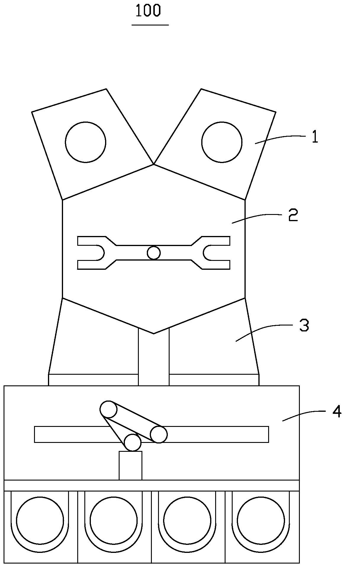
[0031] see figure 1 and figure 2 , in the first embodiment, the semiconductor processing equipment 100 includes a plurality of processing chambers 1 , a transfer chamber 2 , at least one preload chamber 3 , a front-end module 4 and a gas purification device 5 . The multiple processing chambers 1 are used to etch semiconductor wafers, the transfer chamber 2 is used to send the semiconductor wafers into different processing chambers 1, and the pre-loading chamber 3 is used to connect the transfer chambers 2 As well as the front-end module 4 of the equipment, the gas purification device 5 is arranged in the pre-loading chamber 3 . The equipment front-end module 4 is used for sending unprocessed semiconductor wafers into the semiconductor processing equipment 100 , or for sending processed semiconductor wafers out of the semiconductor processing equipment 100 .

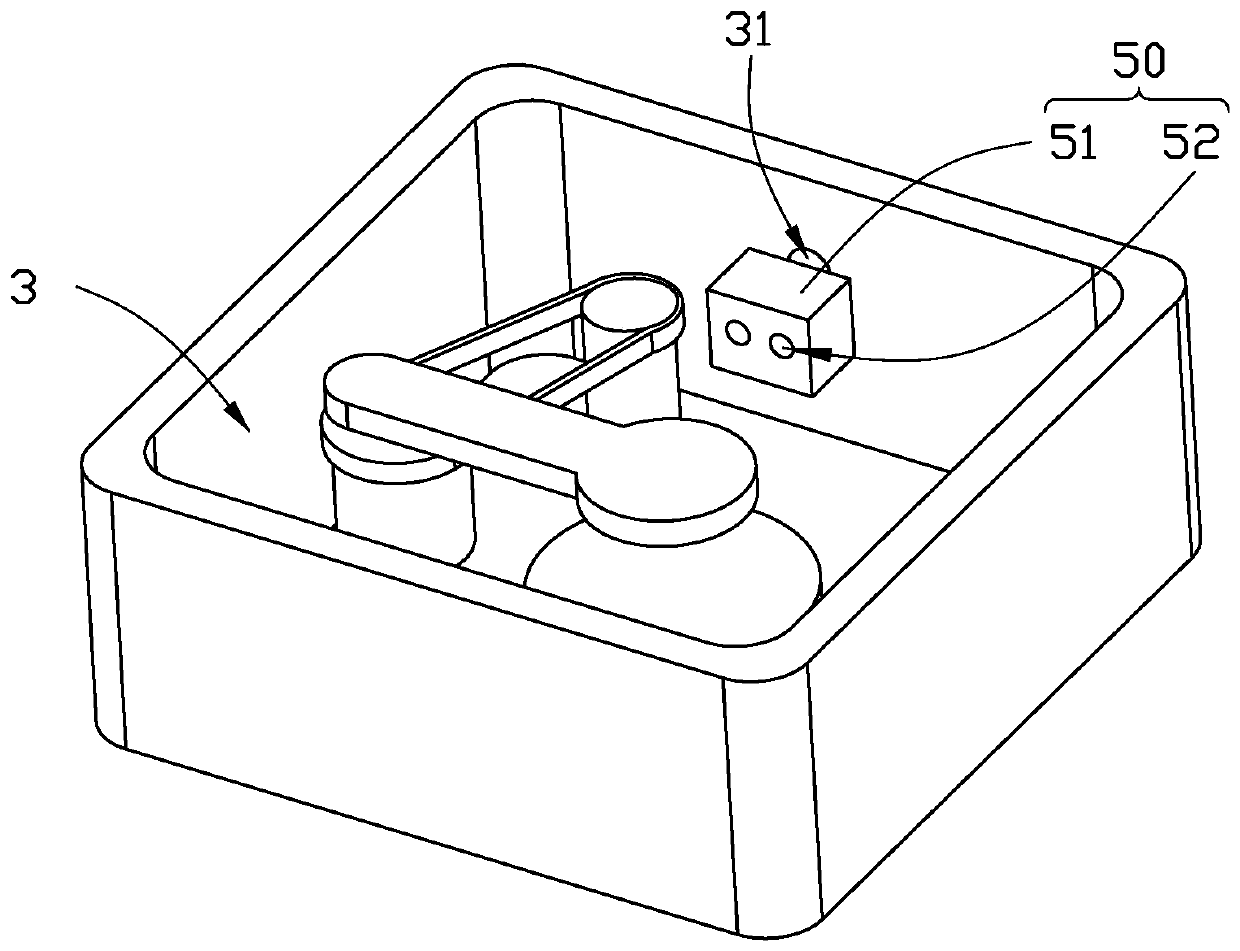
[0032] Further, the pre-loading chamber 3 is connected to a vent pipe 31, and the gas purification device 5 is arran...

no. 2 example

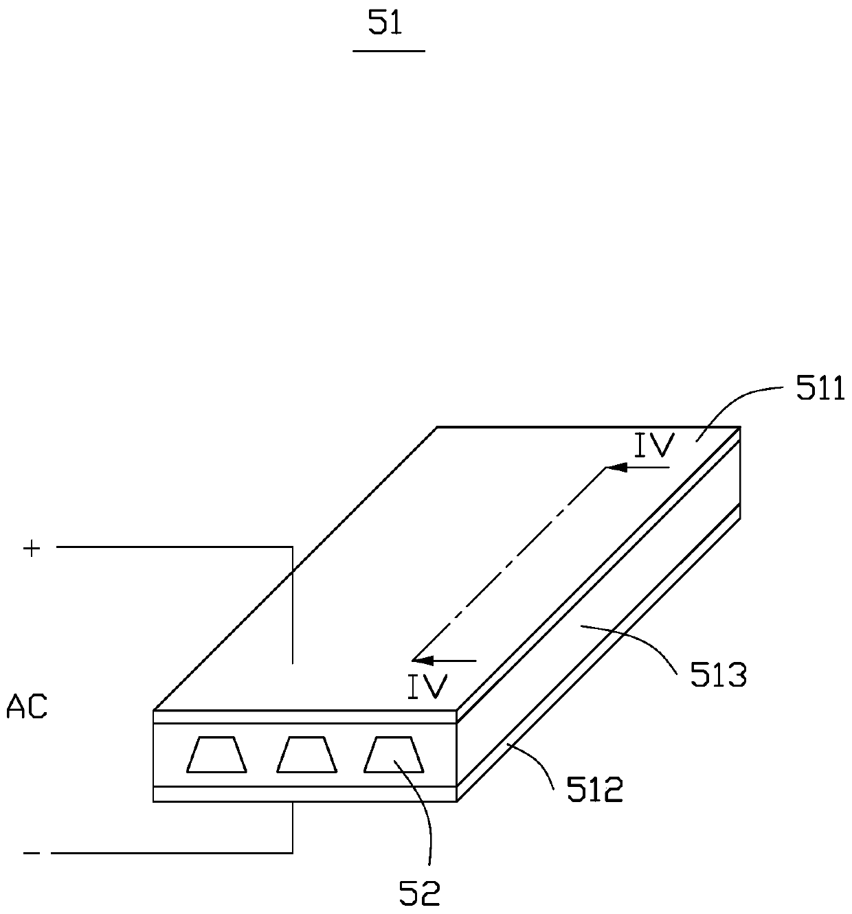
[0039] see figure 1 , figure 2 and Image 6 , the semiconductor processing equipment 100 includes a plurality of processing chambers 1 , a transfer chamber 2 , at least one pre-load chamber 3 , a front-end module 4 and a gas purification device 5 . The multiple processing chambers 1 are used to etch semiconductor wafers, the transfer chamber 2 is used to send the semiconductor wafers into different processing chambers 1, and the pre-loading chamber 3 is used to connect the transfer chambers 2 As well as the front-end module 4 of the equipment, the gas purification device 5 is arranged in the pre-loading chamber 3 . The pre-loading chamber 3 is connected to a vent pipe 31 , and the gas purification device 5 is arranged at the inlet end of the vent pipe 31 , and the gas inlet end is located on the inner cavity side wall of the pre-load chamber 3 . The gas purification device 5 includes a plasma generator 51 and an airflow channel 52 , the airflow channel 52 runs through the ...

no. 3 example

[0043] see Figure 7 The semiconductor processing equipment of the third embodiment is substantially the same as that of the semiconductor processing equipment of the first embodiment, the difference is that the semiconductor processing equipment of the third embodiment further includes a filter 7 . The filter 7 is arranged at the intake end of the vacuum pump 32 to prevent the pollution particles from entering the vacuum pump 32 and ensure the stable and safe operation of the vacuum pump 32 .

[0044] Further, a third detector 8 is also arranged in the inner cavity of the pre-loading chamber 3 , and the third detector 8 is used to detect the particle concentration in the pre-loading chamber 3 . A valve 311 is provided in the ventilation pipe 31 , and the valve 311 is electrically connected to the third detector 8 . When the detection value of the third detector 8 is lower than a preset value, it means that the gas environment in the pre-loading chamber 3 has reached the clea...


PUM


Abstract

The invention provides semiconductor processing equipment, which comprises a processing chamber, an equipment front-end module, a transfer chamber, a front loading chamber and a gas purification device, the front loading chamber is connected with a breather pipe, and the gas purification device is arranged at the gas inlet end of the breather pipe. The gas purification device comprises a plasma generator and a gas flow channel. The gas flow channel penetrates through the plasma generator and is communicated with the front loading chamber and the breather pipe. The pipe diameter of the gas flowchannel is smaller than that of the breather pipe, gas in the front loading chamber naturally flows towards the breather pipe through a Venturi effect, the plasma generator is used for purifying thegas flowing through the gas flow channel, and therefore the purpose of removing pollutants in the front loading chamber is achieved.

Description

technical field [0001] The invention relates to the field of semiconductor manufacturing, in particular to semiconductor processing equipment. Background technique [0002] A loadlock chamber in semiconductor processing equipment is generally used to supply semiconductor wafers to corresponding processing chambers. Semiconductor wafers are produced in processing chambers by etching, thin film deposition, etc. These process steps will generate contaminants such as impurity particles, smoke and dust, and these pollutants are a major concern during the processing of semiconductor wafers by processing equipment . Due to the different pressures between different chambers of semiconductor processing equipment, contaminants are often left in the front-loading chamber, and these pollutants will adhere to the semiconductor wafers entering the front-loading chamber, thereby affecting the process of semiconductor wafers , leading to a decrease in the overall yield of the device. Co...

Claims


Application Information

Patent Timeline
IPC IPC(8): H01J37/32H01L21/67B01D50/00
CPCB01D50/00H01J37/32862H01J2237/334H01J2237/335H01L21/67069
Inventor 金建澔具德滋
Owner XIA TAI XIN SEMICON QING DAO LTD
Why Eureka
Try Eureka