
Printed integrated circuit board forming and manufacturing process

An integrated circuit board and manufacturing process technology, applied in the field of circuit board manufacturing, can solve the problem of the inability to guarantee the bonding effect of patch components and insulating substrates, the inability to guarantee the alignment of patch components on insulating substrates, and the thickness difference between patch components and insulating substrates. and other problems to achieve the effect of improving the paste effect, eliminating air bubbles and improving uniformity

Active Publication Date: 2020-06-30
ANHUI BOTAI CIRCUIT TECH
View PDF4 Cites 2 Cited by
  • Summary
  • Abstract
  • Description
  • Claims
  • Application Information

AI Technical Summary

Problems solved by technology

[0005] The present invention provides a printing integrated circuit board forming process, aiming to solve the following problems in the current manufacturing process of printed integrated circuit boards when manually pasting patch components: (1) Manually use tweezers to pick up the patch components When pasting, due to visual errors and hand shaking, the alignment of the patch components on both sides of the insulating substrate cannot be guaranteed; (2) After the patch components are pasted on the insulating substrate, the red between the patch components and the insulating substrate There are differences in the thickness of the glue, and some air bubbles will remain in the red glue, which cannot guarantee the sticking effect between the patch component and the insulating substrate

Method used


Image

  • Printed integrated circuit board forming and manufacturing process
  • Printed integrated circuit board forming and manufacturing process
  • Printed integrated circuit board forming and manufacturing process

Examples


Embodiment Construction

[0033] The embodiments of the present invention will be described in detail below with reference to the accompanying drawings, but the present invention can be implemented in many different ways defined and covered by the claims.

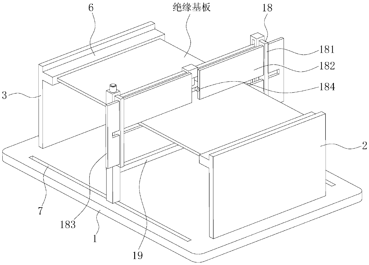
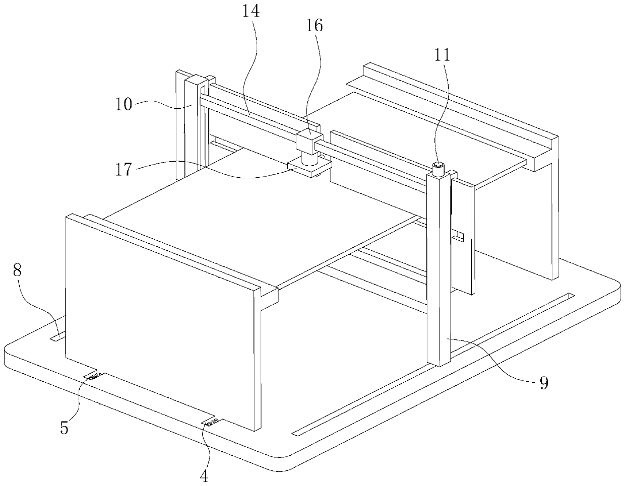
[0034] Such as Figure 2 to Figure 7 As shown, the present embodiment provides a printed integrated circuit board forming and manufacturing mechanical cooperation, including a horizontal bottom plate 1, the upper surface of the bottom plate 1 is vertically installed with a first support plate 2 and a second support plate 3 parallel to each other, the second support plate 3 A support plate 2 is fixedly connected to the upper surface of the base plate 1, and the upper surface of the second support plate 3 and the base plate 1 is slidably connected along a chute 4 perpendicular to the first support plate 2. The first support spring 5 of the plate 2 . On the opposite sides of the first support plate 2 and the second support plate 3, ferrules 6 correspo...


PUM


Abstract

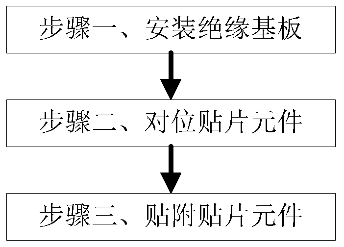
The invention belongs to the technical field of circuit board manufacturing, and particularly relates to a printed integrated circuit board forming and manufacturing process. A printed integrated circuit board forming and manufacturing machine is used in cooperation to complete the process. The process specifically comprises the following steps: step 1, mounting an insulating substrate: insertingtwo ends of the insulating substrate into clamping sleeves to be clamped, step 2, aligning patch elements: coating the upper and lower surfaces of the insulating substrate with red glue, and adjustingthe positions of pasting mechanisms in the horizontal longitudinal direction and the horizontal transverse direction to enable the positions of the two pasting mechanisms to correspond to each other;3, attaching a patch element: mounting the patch element on a pasting mechanism, and pressing the patch element against the red glue on the insulating substrate; and then pasting the patch element through the pasting mechanism. When the printed integrated circuit board forming and manufacturing process is used for pasting the patch elements, the positions of the patch elements on the upper side and the lower side of the insulating substrate can be aligned, the uniformity of the thickness of red glue is improved, and the pasting effect is improved.

Description

technical field [0001] The invention belongs to the technical field of circuit board manufacturing, and in particular relates to a molding and manufacturing process of a printed integrated circuit board. Background technique [0002] Printed integrated circuit boards are one of the important components of the electronics industry, and have been widely used in the production and manufacture of electronic products. The printed circuit board is composed of an insulating base plate, connecting wires and patch components, and has the dual functions of a conductive circuit and an insulating substrate. It can replace complex wiring and realize the electrical connection between components in the circuit, which not only simplifies the assembly work of electronic products, but also reduces the volume of the whole machine, reduces product costs, and improves the quality and reliability of electronic equipment. [0003] During the production process of the printed circuit board, it is ...

Claims


Application Information

Patent Timeline
IPC IPC(8): H05K3/30H05K3/00
CPCH05K3/0008H05K3/303H05K3/305
Inventor 倪敏跃张盼盼张赛
Owner ANHUI BOTAI CIRCUIT TECH
Learn More