
Conductive particles, conductive materials, and contact structures

A technology of conductive particles and conductive layers, applied in the field of conductive materials, contact structures, and conductive particles, can solve the problems of reducing reliability resistance, reducing contact resistance, and difficult to achieve anisotropic conductive material joint resistance, etc., to reduce the initial Resistance, low initial resistance, and improved contact reliability

Active Publication Date: 2021-10-26
DUK SAN NEOLUX
View PDF22 Cites 0 Cited by
  • Summary
  • Abstract
  • Description
  • Claims
  • Application Information

AI Technical Summary

Problems solved by technology

However, the method described above uses only a part of the physical properties of conductive particles, and it is difficult to achieve an efficient junction resistance of anisotropic conductive materials.
[0009] For example, when there are protrusions in the conductive particles and the strength during compression is high, it will help to penetrate the oxide coating of the electrode, but if this is the only way, it is difficult to effectively reduce the thickness of the conductive particles when the strength of the conductive particles is high. Contact resistance while reducing reliability resistance

Method used

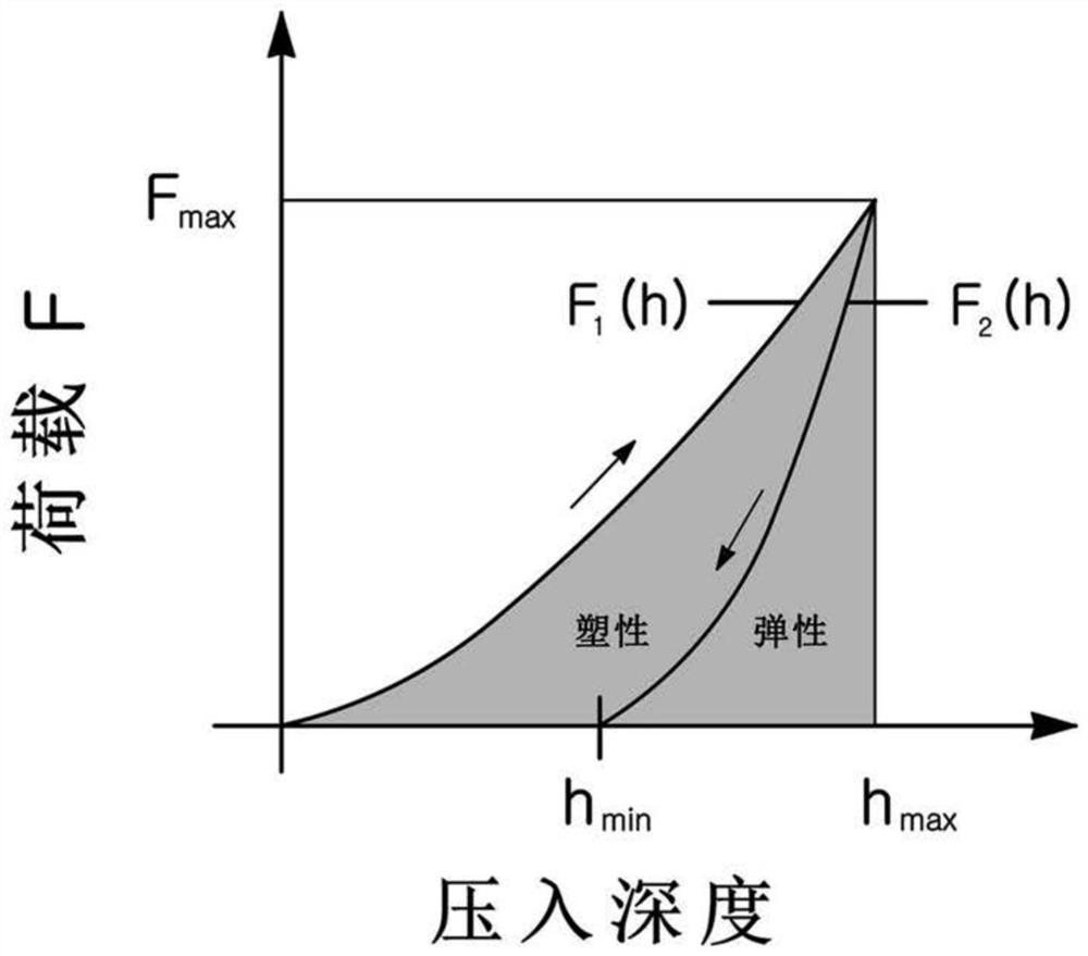

Image

  • Conductive particles, conductive materials, and contact structures
  • Conductive particles, conductive materials, and contact structures
  • Conductive particles, conductive materials, and contact structures

Examples


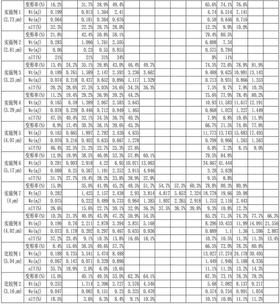
Embodiment 1

[0089] 1) Synthesis of insulator core

[0090] In a 3L glass beaker, 750g of monomer trimethylolpropane ethoxylate triacrylate (TMPETA, Trimethylolpropane ethoxylate triacrylate), 40g of 1,6-hexanediol ethoxylate diacrylate (HDEDA, 1,6- Hexanediol ethoxylate diacrylate) and 750g of divinylbenzene (DVB, Divinylbenzene) and 5g of benzoyl peroxide (BPO) were added and then processed in a 40kHz ultrasonic cleaner (bath) for 10 minutes to prepare the first solution.

[0091] Dissolve 500 g of dispersion stabilizer polyvinylpyrrolidone (PVP, Polyvinylpyrrolidone)-30K and surfactant dioctylsulfosuccinate sodium salt (Solusol, Dioctylsulfosuccinate sodium salt) to 4,000 g in a 5 L polypropylene (PP) beaker deionized water to prepare the second solution.

[0092] After putting the above-mentioned first solution and second solution into a 50L reactor and adding 41,000g of deionized water, they were treated with an ultrasonic homogenizer (Homogeniser, 20kHz, 600W) for 90 minutes, and...

Embodiment 2

[0108] In Example 1 above, 1500 g of 1,6-hexanediol ethoxylate diacrylate (HDEDA) was used to synthesize the insulator core. Using 24 g of the above-fabricated insulator core, the remaining process was performed in the same manner as in Example 1. The average diameter of the insulator core produced above was 2.53 μm. The protrusion size of the above-produced conductive particles was 86 nm.

Embodiment 3

[0110] In Example 1 above, 800 g of trimethylol propane ethoxylate triacrylate (TMPETA), 50 g of 1,6-hexanediol ethoxylate diacrylate (HDEDA) and 800 g of divinylbenzene (DVB) were used Synthesize an insulator core. Using 40 g of the above-produced insulator core, the remaining processes were performed in the same manner as in Example 1. The average diameter of the insulator core produced above was 3.04 μm. The protrusion size of the above-produced conductive particles was 135 nm.


PUM

PropertyMeasurementUnit
thicknessaaaaaaaaaa
diameteraaaaaaaaaa
diameteraaaaaaaaaa

Abstract

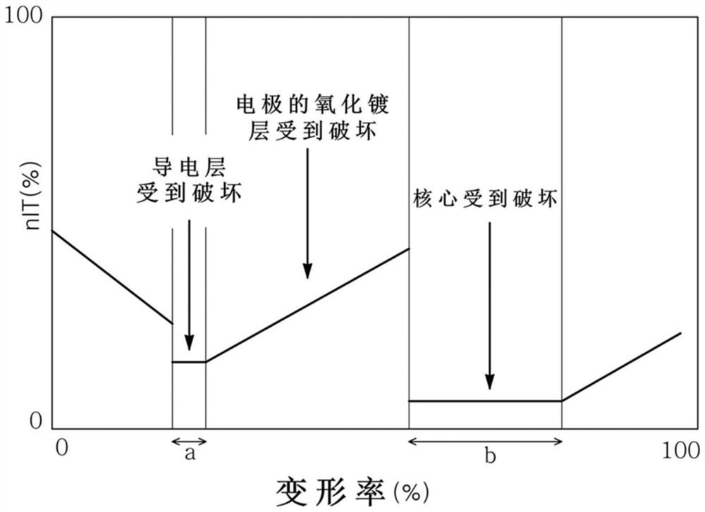
The present invention provides a conductive particle, a conductive material, and a contact structure. The conductive particle is characterized in that: in the conductive particle electrically connected to the electrode by being contained between the electrodes, the conductive particle includes an insulator core, and is equipped with an insulator core. The conductive layer or the conductive layer with protrusions on the surface of the above-mentioned core, after compressing the above-mentioned conductive particles at 25° C. using a micro-pressure tester, the deformation rate of the above-mentioned conductive particles is used as the x-axis and is expressed by the following formula 1 In the graph plotted with the determined elastic work ratio as the y-axis, the interval (a) where a certain elastic work ratio is maintained after the first discontinuity point and the interval (b) where a constant x elastic work ratio is maintained after the second discontinuity point ) within the deformation rate range of the conductive particles, the above-mentioned oxide plating layer is destroyed by the above-mentioned electrode layer or the above-mentioned conductive layer with protrusions [Formula 1] nIT=W elastic / W total *100.

Description

technical field [0001] The present invention relates to a conductive particle that forms a conductive layer on the surface of an insulator core, and more particularly to a conductive particle that is used as a conductor in a conductive material that is mounted on an electrode of a chip of an electronic device and electrically contacts between electrodes of a substrate. Conductive particles, conductive materials and contact structures. Background technique [0002] Conductive particles are suitable for anisotropic conductive materials used in a dispersed form by mixing with hardeners, adhesives, and resin binders, such as anisotropic conductive film (Anisotropic Conductive Film), anisotropic conductive adhesive Anisotropic Conductive Adhesive, Anisotropic Conductive Paste, Anisotropic Conductive Ink, Anisotropic Conductive Sheet, etc. [0003] The above-mentioned anisotropic conductive materials are suitable for FOG (Film on Glass; flexible substrate-glass substrate), COF (C...

Claims


Application Information

Patent Timeline
Patent Type & Authority Patents(China)
IPC IPC(8): H01B5/14H01B1/22H01L23/488
CPCH01B1/22H01B5/14H01L23/488
Inventor 金敬钦郑舜浩金钟兑朴俊奕金泰根林永真李枝原刘泳祚裴仓完
Owner DUK SAN NEOLUX
Learn More