A multifunctional photonic chip detection system

A technology of photonic chip and detection system, which is applied in the field of detection system to achieve the effect of convenient coupling

Active Publication Date: 2022-03-15
TIANJIN UNIV
View PDF13 Cites 0 Cited by
  • Summary
  • Abstract
  • Description
  • Claims
  • Application Information

AI Technical Summary

Problems solved by technology

However, there is no photonic chip detection system that can simulate a variety of measurement environmental parameters (temperature, humidity, gas, air pressure, magnetic field, electric field, and illumination intensity) and measure multiple parameters (optical signals, electrical signals)

Method used


Image

  • A multifunctional photonic chip detection system
  • A multifunctional photonic chip detection system
  • A multifunctional photonic chip detection system

Examples


Embodiment Construction

[0026] The present invention will be described in further detail below in conjunction with the accompanying drawings and specific embodiments. It should be understood that the specific embodiments described here are only used to explain the present invention, not to limit the present invention.

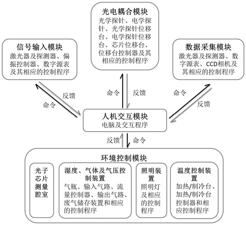
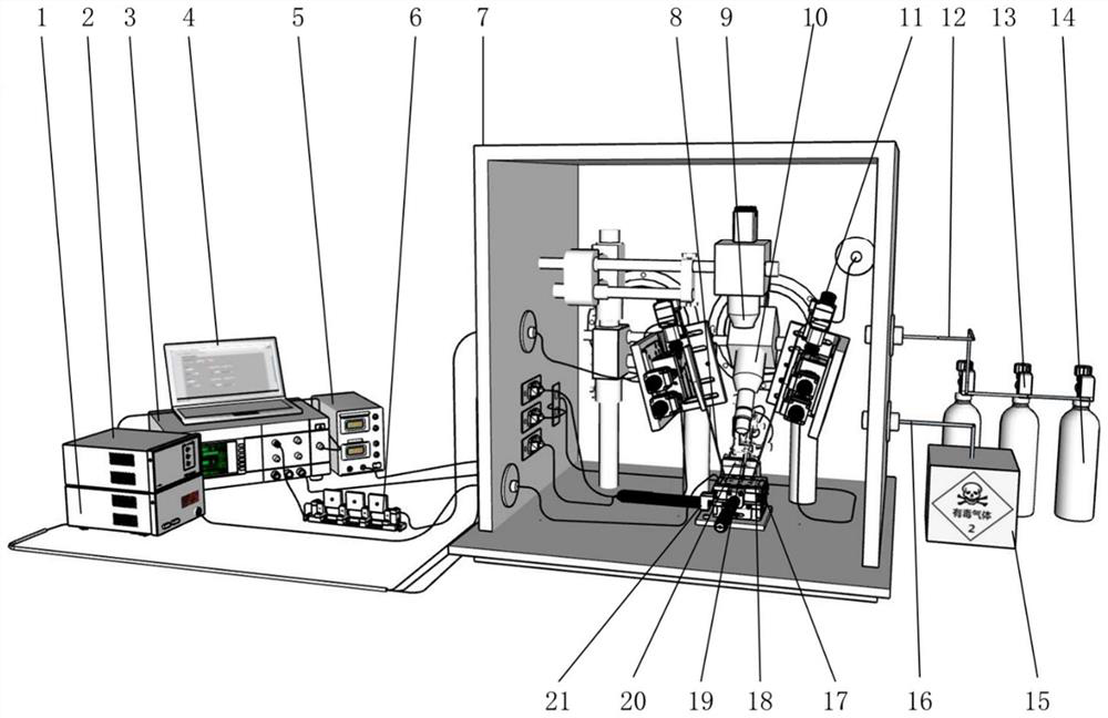
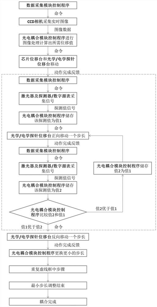
[0027] The multifunctional photonic chip detection system of the present invention is mainly composed of five modules, namely: a signal input module; a photoelectric coupling module; a data acquisition module; an environment control module; and a human-computer interaction module. The signal input module is mainly used to input optical and electrical signals; the photoelectric coupling module is mainly used to couple optical and electrical signals into the chip; the data acquisition module is mainly used to collect the output data of the chip and detect the image information near the chip; the environment control module is mainly used It is used to control the environmental parameters...


PUM


Abstract

The invention discloses a multifunctional photonic chip detection system, which includes five modules: a signal input module is mainly used for inputting optical and electrical signals; a photoelectric coupling module is mainly used for coupling optical and electrical signals into the photonic chip; a data acquisition module is mainly used for It is used to collect the output data of the photonic chip and detect the image information near the photonic chip; the environmental control module is mainly used to control the environmental parameters where the photonic chip is located; the human-computer interaction module is mainly used to realize the dialogue between the human and the multi-functional photonic chip detection system. The system is controlled through an interactive interface, which is convenient and simple. It can realize automatic coupling and manual coupling between optical fiber and photonic chip; it can control various environmental parameters around the chip to meet the needs of different types of photonic chip detection, and can also test various optical and electrical parameters.

Description

technical field [0001] The invention relates to the field of chip detection, in particular to a detection system capable of performing multi-parameter measurement on a photonic chip under various environmental parameters. Background technique [0002] Photonic chips have a very wide range of applications in the fields of optical interconnection, optical communication, biochemical molecular sensing, etc. Therefore, research on photonic chips has received extensive attention in recent years. Compared with traditional electronic chips, photonic chips have unique advantages in many aspects such as communication speed, energy consumption, sensing sensitivity, and anti-electromagnetic interference capabilities, and can be further integrated with electronic devices on a single chip, and finally realized on-chip. A series of functions such as information detection, collection, processing, calculation, and communication. It is foreseeable that photonic chips will have very broad app...

Claims


Application Information

Patent Timeline
Patent Type & Authority Patents(China)
IPC IPC(8): G01D21/02
CPCG01D21/02
Inventor 程振洲武靖雯邢正锟杨凌雁靳喜博任可欣张恒锐胡浩丰刘铁根
Owner TIANJIN UNIV
Why Eureka
Try Eureka