Silicon wafer conveying equipment on sputtering table and using method

A technology for conveying equipment and silicon wafers, which is applied in the directions of conveyor objects, transportation and packaging, sustainable manufacturing/processing, etc. It can solve the problems such as the inability to effectively improve the processing efficiency of silicon wafers and the damage of silicon wafers, so as to improve the processing efficiency of silicon wafers. , The effect of preventing silicon wafer damage and reducing waste of resources

Pending Publication Date: 2020-07-10
SUZHOU SAISEN ELECTRONICS TECH
View PDF0 Cites 5 Cited by
  • Summary
  • Abstract
  • Description
  • Claims
  • Application Information

AI Technical Summary

Problems solved by technology

[0005] The object of the present invention is to provide a silicon wafer conveying device on a sputtering table, which is used to solve the problem in the prior art that the silicon wafer will collide with the conveying device during the conveying process, which may easily cause damage to the silicon wafer and cannot effectively improve the processing efficiency of the silicon wafer. question

Method used


Image

  • Silicon wafer conveying equipment on sputtering table and using method
  • Silicon wafer conveying equipment on sputtering table and using method
  • Silicon wafer conveying equipment on sputtering table and using method

Examples


Embodiment 1

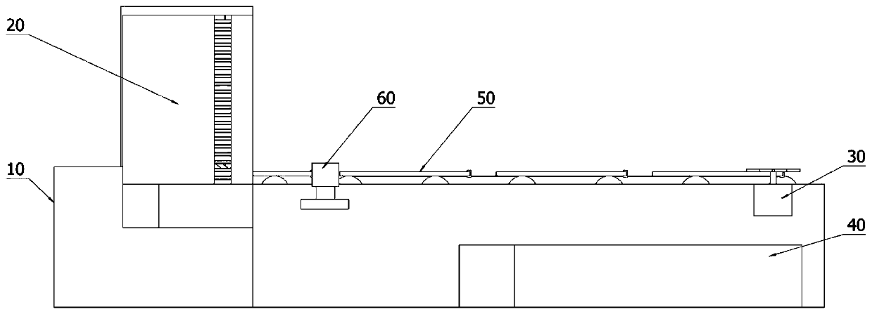
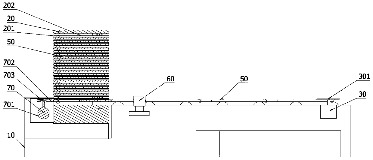
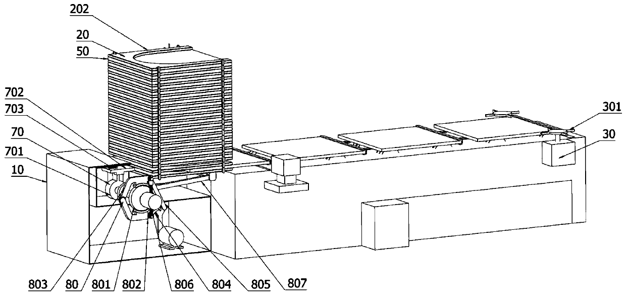
[0050] Such as figure 1 , 2 As shown, this embodiment discloses a silicon wafer 50 conveying device, comprising: a body 10, a placement device 20, a housing 201, a lead-out device 70, a lead-out plate 702, and a driving device 80. The body 10 is arranged on a plane, and the body 10 Inside is provided with delivery wheel 102, delivery wheel 102 is fixedly connected with body 10; placement device 20, placement device 20 is arranged on one side of body 10, placement device 20 is connected with body 10, placement device 20 comprises: shell 201, shell 201 sets Above the body 10, the shell 201 is connected with the body 10, and the inside of the shell 201 is hollow; the plate 202 is placed, and the plate 202 is arranged inside the shell 201, and a gap is provided between the plate 202, and the space of the plate 202 is used To store the silicon wafer 50; the deriving device 70, the deriving device 70 is arranged inside the body 10, the deriving device 70 is fixedly connected with t...


PUM


Abstract

The invention discloses silicon wafer conveying equipment on a sputtering table, and relates to the technical field of silicon wafer processing. According to the silicon wafer conveying equipment on the sputtering table, a machine body is arranged on a plane, conveying wheels are arranged in the machine body, and the conveying wheels are fixedly connected with the machine body; a placing device isarranged on one side of the machine body, is connected with the machine body, and comprises a shell arranged above the machine body, the shell is connected with the machine body in a matched manner,and the interior of the shell is hollow; placing plates are arranged in the shell, and a gap is formed between the placing plates; the guide-out device is arranged in the machine body, is fixedly connected with the machine body, and comprises a guide-out plate arranged in the machine body, the guide-out plate is matched with the gap of the placing plate, and the guide-out plate can be inserted into the gap of the placing plate; and a driving device is arranged in the machine body. The silicon wafer conveying device is used for solving the problem that in the prior art, silicon wafers collide with a conveying device in the conveying process, the silicon wafers are damaged easily, and the silicon wafer machining efficiency cannot be effectively improved.

Description

technical field [0001] The invention relates to the technical field of silicon wafer processing, in particular to a silicon wafer conveying device on a sputtering table and a method for using it. Background technique [0002] At present, solar energy has become a relatively widely used renewable energy source for human beings, and solar cells are the main tool for utilizing solar energy, and their function is to directly convert solar energy into electrical energy. [0003] The conversion efficiency of a solar cell is the ratio of the power generated by the cell to the incident light power. Silicon wafers are the main material of solar cells. In order to improve the conversion efficiency of solar cells, silicon wafers need to be processed or processed in multiple steps. [0004] During the production process of solar silicon wafers, silicon wafers are usually stored in silicon wafer racks, and taken out one by one during production to cooperate with the subsequent productio...

Claims


Application Information

Patent Timeline
Patent Type & Authority Applications(China)
IPC IPC(8): H01L21/677H01L21/203H01L31/18
CPCH01L21/203H01L21/67739H01L31/18Y02P70/50
Inventor 伍志军
Owner SUZHOU SAISEN ELECTRONICS TECH
Why Eureka
Try Eureka