3D NAND memory and manufacturing method thereof

A 3D NAND and manufacturing method technology, applied in the direction of electric solid-state devices, semiconductor devices, electrical components, etc., can solve problems affecting the use of devices, leakage, and limited grid line gap size, so as to improve the yield rate, increase the formation window, reduce The effect of difficulty

Active Publication Date: 2020-07-10
YANGTZE MEMORY TECH CO LTD
View PDF5 Cites 6 Cited by
  • Summary
  • Abstract
  • Description
  • Claims
  • Application Information

AI Technical Summary

Problems solved by technology

[0003] In the 3D NAND process, gate line gaps are usually formed to form stacked gate layers. In order to control the effective gate area, the size of the gate line gaps needs to be limited, thus making the size of the gate line gaps very limited. When the common source is subsequently formed through the gate li...

Method used


Image

  • 3D NAND memory and manufacturing method thereof
  • 3D NAND memory and manufacturing method thereof
  • 3D NAND memory and manufacturing method thereof

Examples


Embodiment 1

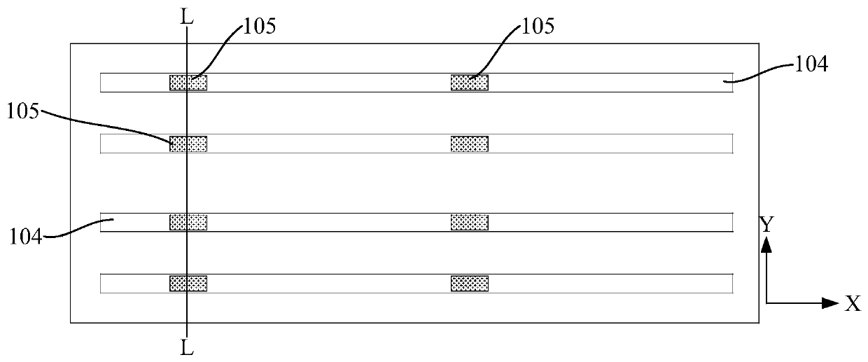
[0115] In the manufacturing process of 3D NAND, it is usually necessary to form a gate line gap, remove and replace the sacrificial layer in the stacked structure through the gate line gap, form a gate layer, and form the common source of the array storage structure at the position of the gate line gap, and then A contact portion of the common source is formed over the common source. refer to figure 1 Considering the size of the device and the area of ​​the gate in the device, the size of the gate line gap and the subsequent common source 104 formed therein is very limited, and the contact portion 105 of the common source should be formed above the common source 104, and the limited The size of the common source electrode limits the formation window of the contact portion 105. Therefore, during the formation of the contact portion 105, if the position of the contact portion 105 is slightly deviated, when it is formed on both sides of the source electrode 104, it is easy to bri...

Embodiment 2

[0142] This embodiment also provides a method for forming a stepped structure of a 3D NAND memory, and the similarities with Embodiment 1 will not be repeated, and the difference lies in:

[0143] Such as Figure 16 As shown, in this embodiment, the first trench 203 is formed in the stacked structure. The first grooves 203 formed in this embodiment are also distributed at intervals in the first direction, and include a first part 2031 and a second part 2032 extending parallel in the X direction and distributed at intervals. The first groove 203 in the Y direction The width is also W, and the first portion 2031 and the second portion 2032 have a separation distance Δd in the Y direction. Such as Figure 16 and 17 As shown, the width W is greater than the width of the gate line gap (that is, the subsequently formed common source 104), and the distance Δd between the first part 2031 and the second part 2032 in the Y direction is smaller than or equal to the gate line gap (that...

Embodiment 3

[0148]This embodiment provides a kind of 3D NAND memory, refer to the attached image 3 ~ attached Figure 12 , the 3D NAND memory includes:

[0149] The substrate 100 has a substrate surface in a first direction and a second direction orthogonal to each other, and a stacked structure is formed on the substrate surface in a third direction perpendicular to the substrate surface , the stack structure includes alternately stacked insulating layers and gate layers;

[0150] A first top selection gate tangent line formed in the top selection gate of the gate layer; in a preferred embodiment, the first top selection gate tangent lines 106 are distributed at intervals in the first direction, and the first top selection gate tangent line The width is greater than the width of the subsequently formed gate line gap.

[0151] a gate line slot extending along the first direction and penetrating the stacked structure in the third direction, the gate line slot passing through the first ...


PUM


Abstract

The invention provides a 3D NAND memory and a manufacturing method thereof. Before a grid line gap is formed, a first part selection grid tangent line is formed at a position where a common source electrode contact part is to be formed; the width of the first top selection grid tangent line is greater than that of the grid line gap, so the formed common source contacts the periphery; the stacked layer is replaced by the insulating material for forming the top selection gate tangent, so that a forming window for forming the contact part of the common source electrode is enlarged, even if the contact part is slightly deviated from the common source electrode, the contact part cannot be in contact with the gate layers on the two sides of the bridging common source electrode, the electric leakage risk of the device is reduced, and the yield of the device is improved. Meanwhile, the forming window of the contact part is enlarged, so that the manufacturing difficulty of the contact part is reduced to a certain extent. In addition, the first top selection gate tangent line and the second top selection gate tangent line can be formed by using the same mask, so that the preparation of the mask and the etching step are saved, and the manufacturing cost of the memory is reduced.

Description

technical field [0001] The invention relates to the field of semiconductor integrated circuit manufacturing, in particular to a 3D NAND memory and a manufacturing method thereof. Background technique [0002] As the feature size of devices in integrated circuits continues to shrink, 3D memory technologies that stack multiple planes of memory cells to achieve greater storage capacity and lower cost per bit are increasingly favored. [0003] In the 3D NAND process, gate line gaps are usually formed to form stacked gate layers. In order to control the effective gate area, the size of the gate line gaps needs to be limited, thus making the size of the gate line gaps very limited. When the common source is subsequently formed through the gate line gap and the contact part of the common source is further formed, the position of the contact part and the common source is slightly deviated, which will cause the contact part to bridge the gate layers on both sides of the common source...

Claims


Application Information

Patent Timeline
IPC IPC(8): H01L27/11565H01L27/1157H01L27/11582
CPCH10B43/10H10B43/35H10B43/27
Inventor 王贝寒徐伟周文斌黄攀夏季
Owner YANGTZE MEMORY TECH CO LTD
Why Eureka
Try Eureka