

Semiconductor detection device and detection method
A detection device, semiconductor technology, applied in the direction of semiconductor/solid-state device testing/measurement, electrical components, circuits, etc., can solve the problem that photoresist films cannot generate effective signals, etc., and achieve easy nonlinear optical signals and easy acquisition. Effect
- Summary
- Abstract
- Description
- Claims
- Application Information
AI Technical Summary
Problems solved by technology
Method used
Image

Examples
Embodiment Construction
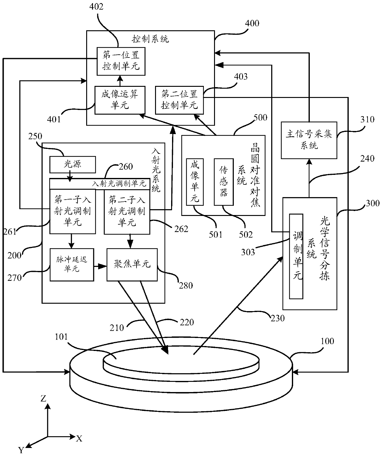
[0038] As mentioned in the background art, realizing real-time detection of molecular-level defects in the manufacturing process is one of the problems to be solved in the field of semiconductor yield detection.
[0039] In order to solve the problem of real-time detection of molecular-level defects in the development and production of advanced semiconductor manufacturing processes due to new materials and process flows, embodiments of the present invention provide a semiconductor detection device and detection method. In the semiconductor detection device, the non-linear optical signal used for detection can be sorted out from the sum-frequency reflected light, so as to characterize the distribution of photochemically active molecules and molecules of the photoresist before exposure or the photoresist after exposure Structural information defects, so as to realize non-destructive detection of molecular-level defects in semiconductor devices.
[0040] In order to make the abov...
PUM
 Abstract
Description
Claims
Application Information