Supercharge Your Innovation With Domain-Expert AI Agents!

Display device

A display device and display device technology, applied in static indicators, optics, instruments, etc., can solve problems such as easy deterioration of liquid crystal devices, and achieve the effects of low power consumption, high display quality, and high reliability

Active Publication Date: 2020-07-14
SEMICON ENERGY LAB CO LTD
View PDF12 Cites 0 Cited by
  • Summary
  • Abstract
  • Description
  • Claims
  • Application Information

AI Technical Summary

Problems solved by technology

In general, liquid crystal devices tend to deteriorate easily when they are constantly supplied with DC voltage

Method used


Image

  • Display device
  • Display device
  • Display device

Examples


Embodiment Construction

[0278] In this example, calculation results of a display device according to one embodiment of the present invention will be described.

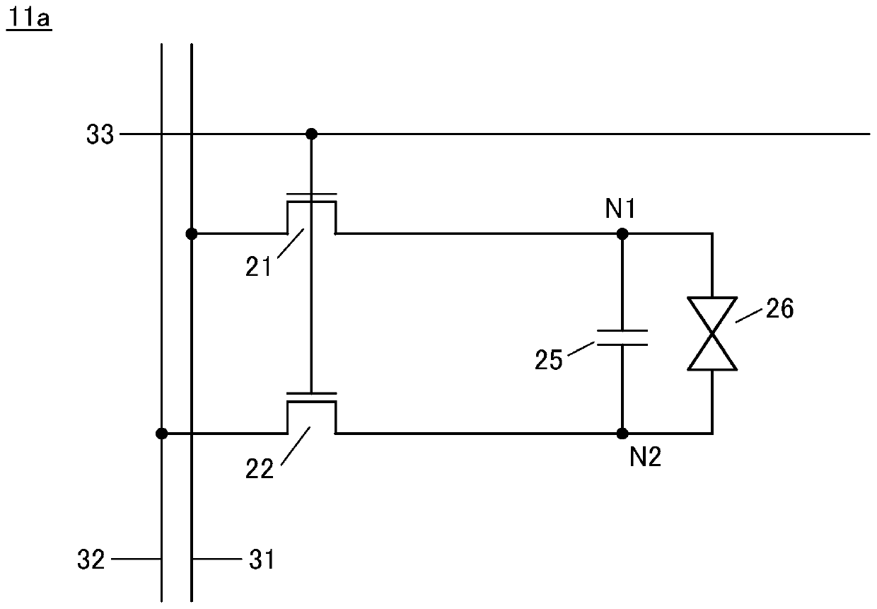
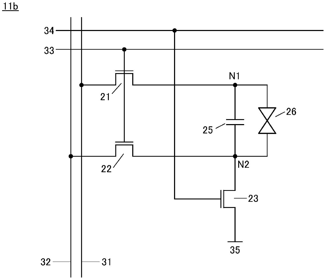
[0279] Figure 15 The structure of the circuit 60 which is the calculation object of this embodiment is shown. Circuit 60 includes pixel 11 , transistor 58 and transistor 59 .

[0280] The pixel 11 is connected to the wiring 31 and the wiring 32 . The wiring 32 is connected to one of the source and the drain of the transistor 58 and to one of the source and the drain of the transistor 59 .

[0281] The other of the source and drain of the transistor 58 is applied with a potential V1, ie, +5V. The other of the source and the drain of the transistor 59 is applied with a potential V2, ie -5V. The gate of transistor 58 is supplied with signal EN. The gate of transistor 59 is supplied with signal ENB. Here, transistor 58 is equivalent to Figure 7A shown as switch 48a or switch 48b, while transistor 59 is equivalent to Figure 7A Either s...


PUM

PropertyMeasurementUnit
sizeaaaaaaaaaa

Abstract

The purpose of the present invention is to provide a display device that has high display quality. The display device has pixels and a source driver circuit. The pixels have first and second transistors (21, 22), a capacitive element (25), and a display element (26). The source drive circuit is electrically connected to first and second wirings (31, 32). The first wiring (31) is electrically connected to one electrode of the capacitive elements (25) and one electrode of the display elements (26) via the first transistors (21). The second wiring (32) is electrically connected to the other electrode of the capacitive elements (25) and the other electrode of the display elements (26) via the second transistors (22).

Description

technical field [0001] One aspect of the present invention relates to a display device and an operating method thereof. [0002] Note that one aspect of the present invention is not limited to the technical fields described above. Examples of the technical field of one aspect of the present invention include semiconductor devices, display devices, light emitting devices, display systems, electronic equipment, lighting devices, input devices (for example, touch sensors, etc.), input and output devices (for example, touch panel, etc.) and a driving method or manufacturing method of the above-mentioned device. [0003] In this specification and the like, a semiconductor device refers to all devices that can operate by utilizing semiconductor characteristics. Display devices (liquid crystal display devices, light-emitting display devices, etc.), projection devices, lighting devices, electro-optical devices, power storage devices, storage devices, semiconductor circuits, imaging ...

Claims


Application Information

Patent Timeline
Patent Type & Authority Applications(China)
IPC IPC(8): G02F1/1368G02F1/133G09G3/20G09G3/36
CPCG02F1/1368G02F1/133G09G3/3688G09G3/20G09G3/36G02F1/13624G09G3/3648G09G3/3614G02F1/134372G09G3/3677H01L27/1255G09G2300/0809H01L27/1225H01L27/124H01L29/24G09G2310/06G09G2300/0426H01L29/7869
Inventor 川岛进楠纮慈高桥圭丰高耕平渡边一德小野谷茂
Owner SEMICON ENERGY LAB CO LTD
Features
  • R&D
  • Intellectual Property
  • Life Sciences
  • Materials
  • Tech Scout
  • Unparalleled Data Quality
  • Higher Quality Content
  • 60% Fewer Hallucinations
Learn More