Check patentability & draft patents in minutes with Patsnap Eureka AI!

Array substrate and display device

A technology for array substrates and display areas, which is applied in instruments, nonlinear optics, optics, etc., can solve the problems of lower display product yield, uneven diffusion of rubbed orientation shadow liquid crystal, bright and dark areas, etc., to improve product yield and display effect, avoid the problem of uneven liquid crystal diffusion, and reduce the effect of friction weak area

Active Publication Date: 2022-07-26
BOE TECH GRP CO LTD +1
View PDF7 Cites 0 Cited by
  • Summary
  • Abstract
  • Description
  • Claims
  • Application Information

AI Technical Summary

Problems solved by technology

[0003] But at present, the inventors have found in the research process that under the influence of the peripheral wiring area, the periphery of the display area in TFT-LCD is prone to friction orientation shadows and uneven liquid crystal diffusion, which makes the periphery of the display area unable to display normally. Bad conditions such as light leakage in the surrounding dark state or dark areas in the bright state reduce the yield of display products

Method used


Image

  • Array substrate and display device
  • Array substrate and display device
  • Array substrate and display device

Examples


Embodiment Construction

[0049] The technical solutions of the present disclosure will be further described in detail below through the embodiments and in conjunction with the accompanying drawings. In the specification, the same or similar reference numerals refer to the same or similar parts. The following description of the embodiments of the present disclosure with reference to the accompanying drawings is intended to explain the general inventive concept of the present disclosure, and should not be construed as a limitation of the present disclosure.

[0050] Furthermore, in the following detailed description, for convenience of explanation, numerous specific details are set forth in order to provide a thorough understanding of the disclosed embodiments. Obviously, however, one or more embodiments may be practiced without these specific details.

[0051]It should be noted that "on", "formed on" and "disposed on" described herein may mean that one layer is directly formed or disposed on another l...


PUM


Abstract

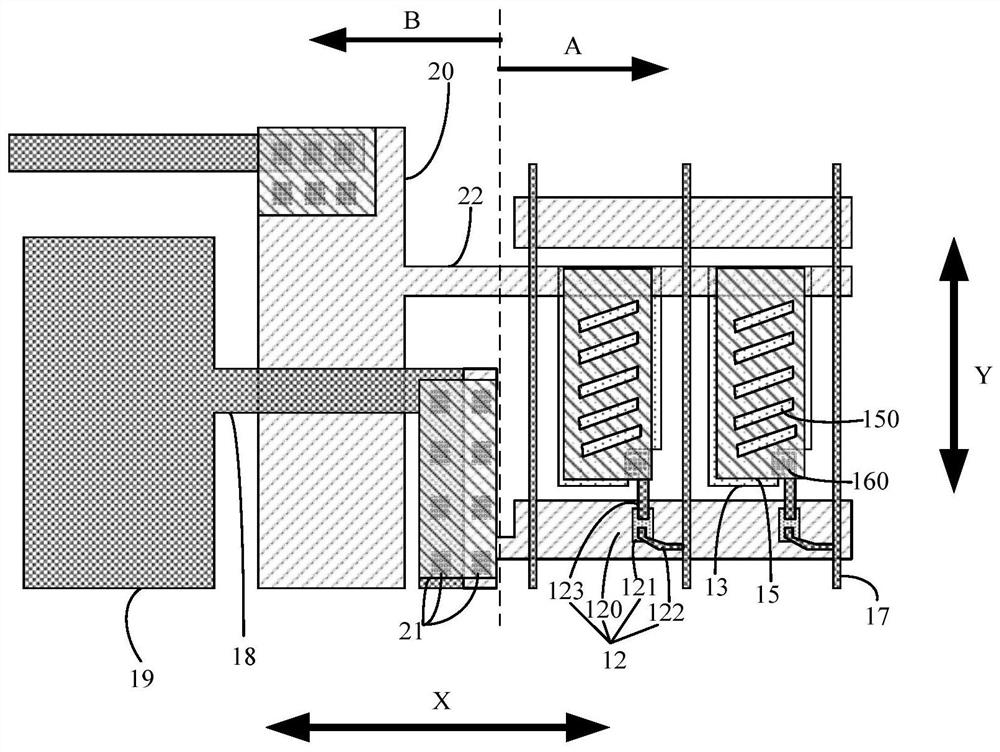
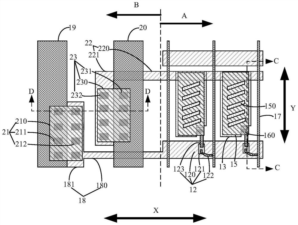
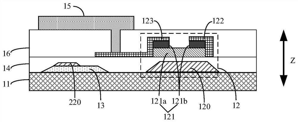
The present disclosure relates to the field of display technology, and in particular, to an array substrate and a display device. The array substrate has a display area and a peripheral wiring area arranged on at least one side of the display area, the display area includes thin film transistors and common electrodes formed on a base substrate; the peripheral wiring area includes a first a lead, a gate signal line and a common signal line; the first lead and the gate of the thin film transistor are arranged in the same layer and are electrically connected to the gate; the gate signal line is located on the side of the first lead away from the base substrate, and passes through the A transfer structure is electrically connected with the first lead; the common signal line is located on the side of the first lead away from the base substrate, and on the side of the gate signal line close to the display area, and the common signal line is electrically connected with the common electrode; wherein, The first switching structure is located on the side of the common signal line away from the display area. This solution improves the display product yield.

Description

technical field [0001] The present disclosure relates to the field of display technology, and in particular, to an array substrate and a display device. Background technique [0002] With the continuous development of display technology, Thin Film Transistor Liquid Crystal Display (TFT-LCD for short) has occupied a dominant position in the field of flat panel display. [0003] However, at present, the inventor found in the research process that under the influence of the peripheral wiring area, the periphery of the display area in the TFT-LCD is prone to rubbing alignment shadows and uneven liquid crystal diffusion, so that the periphery of the display area cannot be displayed normally. Bad conditions such as surrounding dark-state light leakage or bright-state dark areas reduce the display product yield. [0004] It should be noted that the information disclosed in the above Background section is only for enhancement of understanding of the background of the present disclo...

Claims


Application Information

Patent Timeline
Patent Type & Authority Patents(China)
IPC IPC(8): G02F1/1362G02F1/1368G02F1/1343G02F1/1345
CPCG02F1/1362G02F1/136286G02F1/1368G02F1/134363G02F1/13452G02F1/134372
Inventor 黄建华赵重阳孙志华缪应蒙曲莹莹
Owner BOE TECH GRP CO LTD
Features
  • R&D
  • Intellectual Property
  • Life Sciences
  • Materials
  • Tech Scout
  • Unparalleled Data Quality
  • Higher Quality Content
  • 60% Fewer Hallucinations
Learn More