Supercharge Your Innovation With Domain-Expert AI Agents!

Growth method of light-emitting diode epitaxial wafer and light-emitting diode epitaxial wafer

A technology of light-emitting diodes and growth methods, which is applied in the field of light-emitting diode epitaxial wafers, can solve the problems of reducing LED luminous efficiency and affecting the recombination of electrons and holes to emit light, and achieve the effects of facilitating recombined light emission, offsetting stress, and improving luminous efficiency

Active Publication Date: 2020-08-28
HC SEMITEK SUZHOU
View PDF4 Cites 0 Cited by
  • Summary
  • Abstract
  • Description
  • Claims
  • Application Information

AI Technical Summary

Problems solved by technology

[0004] There is a large lattice mismatch between the sapphire substrate and the GaN-based material, and the line defects generated by the lattice mismatch will extend to the active layer, affecting the recombination of electrons and holes and reducing the luminous efficiency of LEDs

Method used


Image

  • Growth method of light-emitting diode epitaxial wafer and light-emitting diode epitaxial wafer
  • Growth method of light-emitting diode epitaxial wafer and light-emitting diode epitaxial wafer
  • Growth method of light-emitting diode epitaxial wafer and light-emitting diode epitaxial wafer

Examples


Embodiment Construction

[0035] In order to make the purpose, technical solution and advantages of the present disclosure clearer, the implementation manners of the present disclosure will be further described in detail below in conjunction with the accompanying drawings.

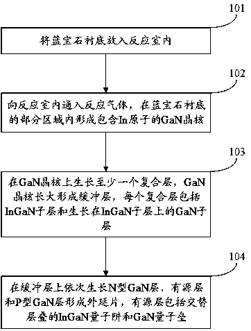
[0036] In the manufacturing process of LED, a semiconductor film is first grown on a single crystal material with a matching crystal structure to form an epitaxial wafer; then electrodes for injecting current are arranged on the epitaxial wafer to form a chip. In related technologies, LED epitaxial wafers include a sapphire substrate, a GaN buffer layer, an N-type GaN layer, an active layer in which InGaN quantum wells and GaN quantum barriers are alternately stacked on the sapphire substrate, and a P-type GaN layer. Among them, when the GaN buffer layer grows, Ga atoms and N atoms gradually grow into GaN crystal nuclei in some regions of the sapphire substrate, and subsequently deposited GaN grows laterally between the GaN crystal ...


PUM

PropertyMeasurementUnit
heightaaaaaaaaaa
thicknessaaaaaaaaaa
thicknessaaaaaaaaaa

Abstract

The disclosure provides a growth method of a light-emitting diode epitaxial wafer and a light-emitting diode epitaxial wafer, which belong to the technical field of semiconductors. The growth method includes: placing a sapphire substrate into a reaction chamber; introducing a reaction gas into the reaction chamber to form a GaN crystal nucleus containing In atoms in a part of the sapphire substrate; grow at least one composite layer on the above, the GaN crystal nucleus grows to form a buffer layer, each of the composite layers includes an InGaN sub-layer and a GaN sub-layer grown on the InGaN sub-layer; growing on the buffer layer in turn The N-type GaN layer, the active layer and the P-type GaN layer form an epitaxial sheet, and the active layer includes alternately stacked InGaN quantum wells and GaN quantum barriers. The present disclosure effectively counteracts the stress generated by the lattice mismatch between the sapphire substrate and the GaN-based material by forming a bulky and stable GaN crystal nucleus.

Description

technical field [0001] The disclosure relates to the technical field of semiconductors, in particular to a method for growing an epitaxial wafer of a light emitting diode and the epitaxial wafer of a light emitting diode. Background technique [0002] Light Emitting Diode (English: Light Emitting Diode, referred to as: LED) is a semiconductor electronic component that can emit light. As an efficient, environmentally friendly and green new solid-state lighting source, LED is a new generation of light source with broad prospects, and is being rapidly and widely used in traffic lights, car interior and exterior lights, urban landscape lighting, indoor and outdoor display screens and small-pitch displays. screen and other fields. [0003] The epitaxial wafer is the primary product in the LED manufacturing process. In related technologies, LED epitaxial wafers include a sapphire substrate, a GaN buffer layer, an N-type GaN layer, an active layer in which InGaN quantum wells and...

Claims


Application Information

Patent Timeline
Patent Type & Authority Patents(China)
IPC IPC(8): H01L33/00H01L33/06H01L33/12
CPCH01L33/007H01L33/06H01L33/12
Inventor 姚振从颖董彬忠李鹏
Owner HC SEMITEK SUZHOU
Features
  • R&D
  • Intellectual Property
  • Life Sciences
  • Materials
  • Tech Scout
  • Unparalleled Data Quality
  • Higher Quality Content
  • 60% Fewer Hallucinations
Learn More