Process for improving ink in high aspect ratio Via hole
A high aspect ratio, ink technology, used in printed circuits, electrical components, printed circuit manufacturing, etc., can solve the problems of ink color limitation, reduce the development line speed, increase the development pressure, etc., to improve the poor ink, simple operation, The effect of simple process
- Summary
- Abstract
- Description
- Claims
- Application Information
AI Technical Summary
Problems solved by technology
Method used
Image
Examples
Embodiment 1
[0022] A process for improving the ink in Via holes with high aspect ratio, the minimum aperture of Via holes is 0.2mm, and the plate thickness is 1.6mm, including the following process steps:
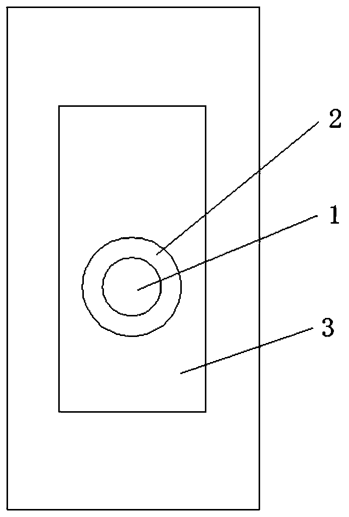
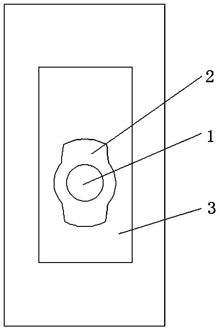
[0023] a. Block design on the screen: the solder mask printing stop is 5mil larger than the Via hole unilaterally (through experimental verification, more than 5mil printing stop will produce SCUM) design, and avoid the solder mask exposure window 3mil safety distance, which is insufficient Cut the solder mask printing stop, such as figure 2 As shown, the aperture of Via hole 1 is 0.2 mm, and the radius of solder mask printing stop 2 is 5 mil larger than that of Via hole 1. At this time, the distance between solder mask printing stop 2 and the short side of solder mask exposure window 3, that is, the left and right is less than 3mil, the two sides of the solder mask printing stop 2 are cut inward to form irregular solder mask printing stop 2 that protrudes up and down;
[0024] b. Sc...
Embodiment 2
[0029] A process for improving the ink in Via holes with high aspect ratio, the minimum aperture of Via holes is 0.2mm, and the plate thickness is 1.8mm, including the following process steps:
[0030] a. Block design on the screen: the solder mask printed stop is designed to be 4.5mil larger than the one side of the Via hole, and the window is 2.5mil safe to avoid solder mask exposure, and the solder mask printed stop is cut off if it is insufficient;
[0031] b. Screen production: select 110-mesh screen;
[0032] c. Anti-soldering pre-treatment: After the pre-treatment ultrasonic washing section, the vibration frequency is controlled at 25Hz to ensure that there is no foreign matter in the hole with a diameter of less than or equal to 0.25mm, and the line speed is 2.5m / min;
[0033] d. Solder resist printing: the printing squeegee and the ink knife are splayed, the printing speed is controlled at 3 / min, the angle of the printing squeegee is controlled at 10°, and the pressur...
Embodiment 3
[0036] A process for improving the ink in Via holes with high aspect ratio, the minimum aperture of Via holes is 0.2mm, and the plate thickness is 2.0mm, including the following process steps:
[0037] a. Block design on the screen: the solder mask printing stop is designed to be 4mil larger than the one side of the Via hole, and the window is 3.5mil safe to avoid solder mask exposure, and the printing stop is cut off if it is insufficient;
[0038] b. Screen production: choose a 90-mesh screen, and its theoretical upper and lower ink volume is 56 cm 2 / m 2 , can meet the ink thickness required by the product, and the wire diameter is 80um at the same time. The irregular solder mask printing stop has no floating area on the screen, and the irregular solder mask printing stop does not fall off;
[0039] c. Pre-treatment for anti-soldering: Washing after the pre-treatment ultrasonic washing section, the vibration frequency is controlled at 26Hz, to ensure that there is no forei...
PUM
 Abstract
Description
Claims
Application Information

