Array substrate, display panel with array substrate and display device

A technology for array substrates and display panels, applied to optics, instruments, electrical components, etc., can solve the problems of poor display quality and low charging rate, and achieve the effects of improving the effect, increasing the charging rate, and shortening the falling time

Inactive Publication Date: 2020-08-07
SHENZHEN CHINA STAR OPTOELECTRONICS SEMICON DISPLAY TECH CO LTD
View PDF4 Cites 5 Cited by
  • Summary
  • Abstract
  • Description
  • Claims
  • Application Information

AI Technical Summary

Problems solved by technology

[0005] Therefore, it is necessary to provide an array substrate, a display panel having the array substrate, and a display device to solve the problem of poor display quality effect caused by the low charging rate of each sub-pixel electrode in the existing display panel and display device. question

Method used


Image

  • Array substrate, display panel with array substrate and display device
  • Array substrate, display panel with array substrate and display device
  • Array substrate, display panel with array substrate and display device

Examples


Embodiment Construction

[0022] The following will clearly and completely describe the technical solutions in the embodiments of the present invention with reference to the drawings in the embodiments of the present invention. Apparently, the described embodiments are some, but not all, embodiments of the present invention. Based on the embodiments of the present invention, all other embodiments obtained by persons of ordinary skill in the art without making creative efforts belong to the protection scope of the present invention.

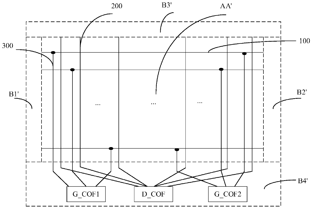
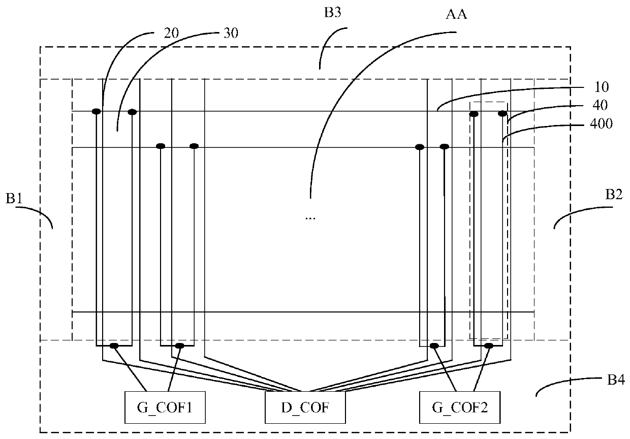
[0023] figure 2 A schematic diagram of the wiring in the array substrate provided for the embodiment of the present invention, as shown in figure 2 As shown, the array substrate is divided into a display area AA and a non-display area surrounding the display area AA, wherein the non-display area includes a left frame B1, a right frame B2, an upper frame B3 and a lower frame B4.

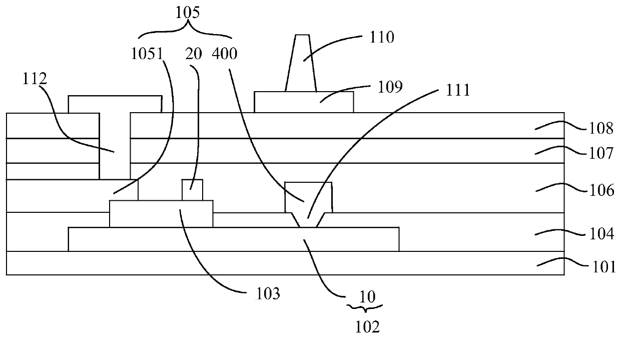
[0024] A plurality of scan lines 10 and a plurality of data lines 20 are arranged in the d...


PUM


Abstract

The invention provides an array substrate. A plurality of scanning lines and a plurality of data lines are arranged in a display area of the array substrate, all the scanning lines are spaced from oneanother and extend along a first direction, all the data lines are mutually spaced and extend along a second direction, and all the scanning lines and all the data lines are insulated and crossed. Aplurality of patch cord units are also arranged in the display area, each patch cord unit comprises at least two patch cords connected in parallel, and all the patch cords are spaced from one anotherand extend along the second direction. Each scanning line corresponds to at least one patch cord unit, each scanning line is connected with all the patch cords in all the corresponding patch cord units, and each patch cord is used for inputting scanning signals to the connected scanning lines. According to the array substrate provided by the invention, the resistance of each patch cord unit is smaller, and the descending time of scanning signals can be greatly shortened, so that the charging rate of each sub-pixel electrode is improved, and the effect of displaying the image quality is furtherimproved. The invention further provides a display panel with the array substrate and a display device.

Description

technical field [0001] The present invention relates to the field of display technology, in particular to an array substrate, a display panel with the array substrate, and a display device. Background technique [0002] At present, manufacturing liquid crystal display panels with large size, high resolution and ultra-narrow bezel has become a development trend of the display panel industry. A liquid crystal display panel generally includes an array substrate, a color filter substrate, and a liquid crystal layer distributed between the array substrate and the color filter substrate. [0003] figure 1 It is a schematic diagram of wiring in the array substrate in the prior art, such as figure 1 As shown, the array substrate is divided into a display area AA' and a non-display area surrounding the display area AA'. Among them, the display area AA' is provided with a plurality of scanning lines 100 extending in the horizontal direction, a plurality of data lines 200 extending ...

Claims


Application Information

Patent Timeline
Patent Type & Authority Applications(China)
IPC IPC(8): G02F1/1362G02F1/1345H01L27/12
CPCG02F1/136286G02F1/13452H01L27/124G02F1/13629
Inventor 朱静
Owner SHENZHEN CHINA STAR OPTOELECTRONICS SEMICON DISPLAY TECH CO LTD
Why Eureka
Try Eureka