A high-precision etching transfer method for micro-nano structure patterns on curved substrates
What is AI technical title?
AI technical title is built by Patsnap AI team. It summarizes the technical point description of the patent document.
A micro-nano structure, high-precision technology, applied in the direction of micro-structure technology, micro-structure devices, manufacturing micro-structure devices, etc., can solve the problem of poor uniformity of etching depth and other problems
Active Publication Date: 2022-03-29
INST OF OPTICS & ELECTRONICS - CHINESE ACAD OF SCI
View PDF3 Cites 0 Cited by
Summary
Abstract
Description
Claims
Application Information
AI Technical Summary
This helps you quickly interpret patents by identifying the three key elements:
Problems solved by technology
Method used
Benefits of technology
Problems solved by technology
[0005] The invention aims at the problem of poor etching depth uniformity in the preparation process of the micro-nano structure pattern of the curved surface substrate of quartz and silicon materials, and proposes a curved surface substrate etching method, which can prepare curved surface microstructures with good etching depth uniformity. nanostructure graphics
Method used
Image
Click on the blue label to locate the original text in one second.
Reading with bidirectional positioning of images and text.
Examples
Embodiment 1
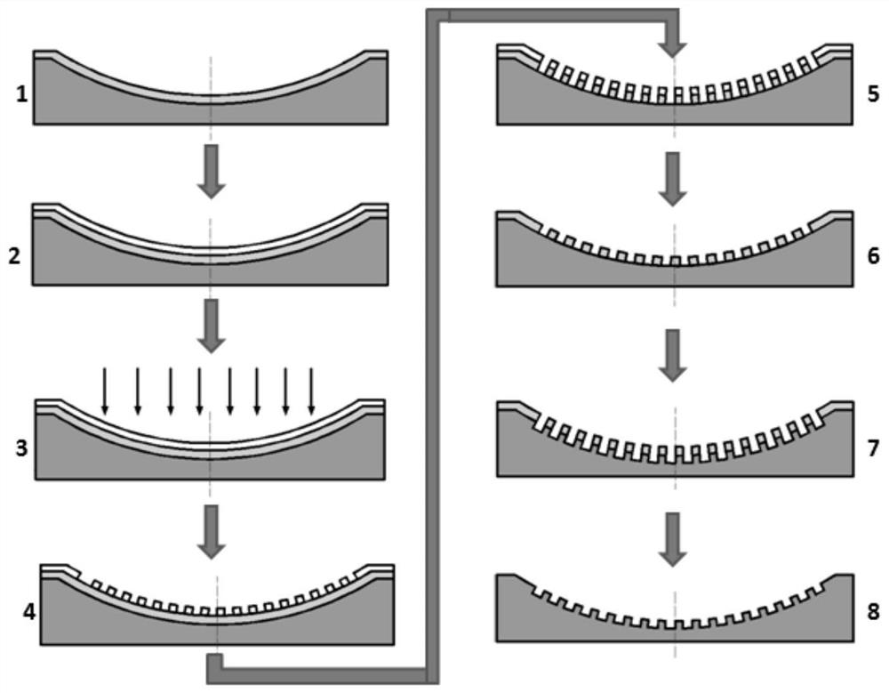
[0051] A high-precision reactive ion etching transfer method for micro-nano structure patterns on a curved substrate of quartz material, the specific steps are as follows:
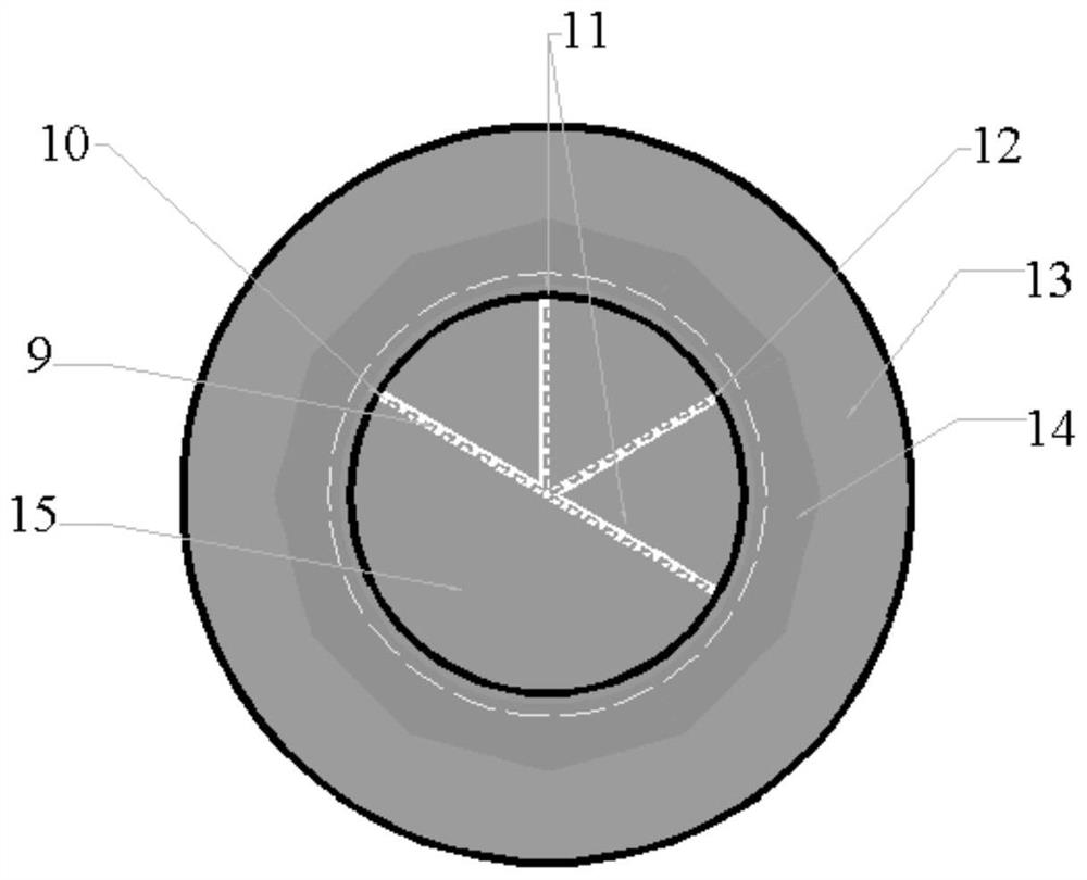
[0052] Step (1), using magnetron sputtering on the curved substrate of concave quartz material, deposits a 100 nanometer thick Cr film; the conductive film 15 in the step (1) is a Cr film;
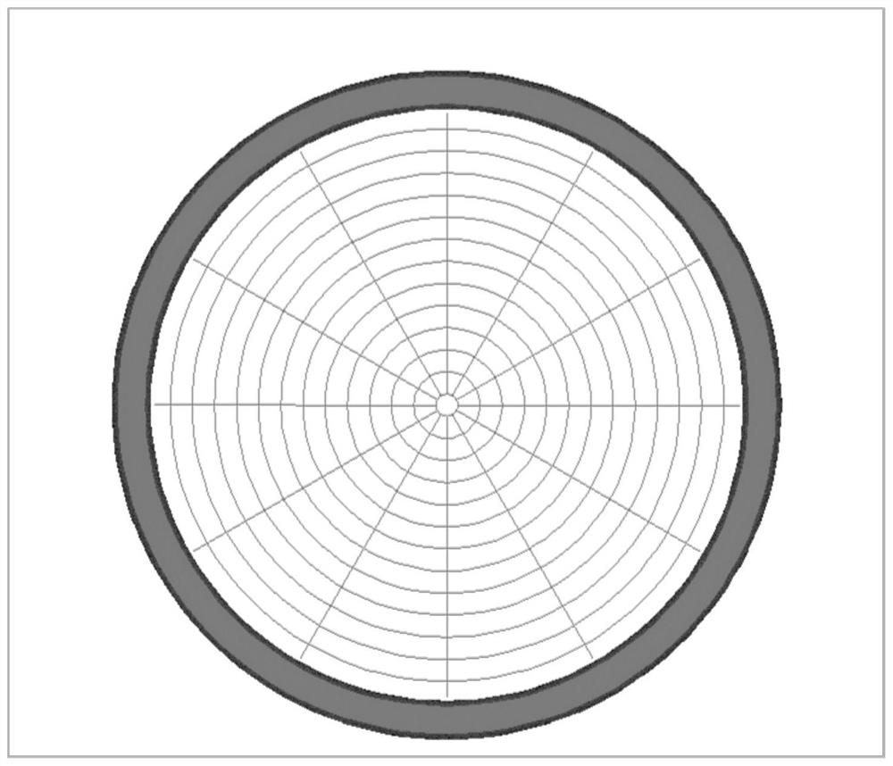
[0053] Step (2), prepare a layer of photoresist with glue coating equipment on the curved surface substrate of the quartz material coated with Cr thin film, and then prepare a predetermined photoresist on the Cr thin film on the curved surface substrate by photolithography. Resist microstructure pattern---a concentric ring array with radial connecting lines;
[0054] Step (3), by using the method of chromium removal liquid wet etching, the photoresist pattern etching is transferred to the Cr conductive film on the curved substrate, forming a Cr film microstructure pattern consistent with the photoresist layer , as a m...
Embodiment 2
[0060] A high-precision reactive ion etching transfer method for a micro-nano structure pattern on a silicon curved substrate, using an electron beam to evaporate an Au film on a convex silicon curved substrate, the specific steps are as follows:
[0061] Step (1), using an electron beam to deposit an Au film with a thickness of 5 nanometers on the curved substrate of the convex silicon material;
[0062] Step (2), prepare a layer of photoresist with glue coating equipment on the silicon curved substrate coated with Au film, and then prepare it on the conductive Au thin film on the convex silicon material curved substrate by laser direct writing method Produce a predetermined photoresist microstructure pattern, such as a network structure with a period of 50 microns;
[0063] Step (3), by ion beam etching, the photoresist pattern etching is transferred to the Au conductive film on the silicon curved substrate to form the Au conductive film microstructure pattern consistent wit...
PUM
Abstract
The invention relates to a high-precision etching transfer method for micro-nano structure patterns on a curved substrate. Using methods such as vacuum thermal evaporation and magnetron sputtering deposition, a layer of conductive film is prepared on the surface of curved substrates made of quartz, silicon, etc., and then through glue coating, photolithography, direct writing, wet etching or dry etching The patterned conductive film consistent with the microstructure pattern is prepared by etching and other processes, and then the conductive film layer around the curved substrate is connected to the lower electrode of the sample stage by using the metal shell and conductive tape to ensure good conductive contact and form an equipotential body. Reactive ion etching is then performed. The method can ensure that the potential of the etching area on the curved substrate is consistent, so that the exposed area of the entire curved substrate is uniformly etched, and the area covered by the metal conductive film is protected. The patterned metal thin film in the invention is not only a mask but also an electrode, which solves the problem of uneven etching transmission of micro-nano structure patterns on curved substrates of dielectric materials such as quartz and silicon.
Description
technical field [0001] The invention relates to the field of preparation of nano-microstructures on curved substrates, in particular to a high-precision etching transfer method for micro-nano structure patterns on curved substrates. Background technique [0002] Diffractive optical elements such as Fresnel lenses, diffraction gratings, and holographic gratings mainly use the diffraction microstructure on the surface of the device to modulate the phase, amplitude, and polarization of light waves to achieve beam smoothing, focusing, collimation, beam splitting, and beam combining. Function. Compared with traditional optical components, the diffractive optical system has the characteristics of high integration, multiple functions, small size, and light weight. Restricted by the processing capacity, most of the diffractive optical elements currently use flat substrates, while the curved substrate diffractive optical elements are mostly used in the infrared band that does not re...
Claims
Application Information
Patent Timeline
Application Date:The date an application was filed.
Publication Date:The date a patent or application was officially published.
First Publication Date:The earliest publication date of a patent with the same application number.
Issue Date:Publication date of the patent grant document.
PCT Entry Date:The Entry date of PCT National Phase.
Estimated Expiry Date:The statutory expiry date of a patent right according to the Patent Law, and it is the longest term of protection that the patent right can achieve without the termination of the patent right due to other reasons(Term extension factor has been taken into account ).
Invalid Date:Actual expiry date is based on effective date or publication date of legal transaction data of invalid patent.

