Spherical vertical micro LED and manufacturing method thereof, display panel and transfer method thereof

A miniature and spherical technology, applied in semiconductor/solid-state device manufacturing, electrical components, electrical solid-state devices, etc., can solve problems such as limiting transfer yield and production efficiency, difficulty in MicroLED, and inability to embed MicroLED, so as to improve transfer yield and Productivity, easy precision registration, low brightness and contrast effects

Pending Publication Date: 2020-08-14
CHONGQING KONKA PHOTOELECTRIC TECH RES INST CO LTD
View PDF0 Cites 7 Cited by
  • Summary
  • Abstract
  • Description
  • Claims
  • Application Information

AI Technical Summary

Problems solved by technology

[0004] However, the Micro LEDs in the prior art are all cuboid or cylindrical structures. When the Micro LEDs fall onto the loading wells on the substrate, due to the limitation of their structure, it is difficult for the Micro LEDs to be precisely aligned with the loading wells on the substrate. , it is prone to the problem that Micro LED cannot be embedded in the loading well, which greatly limits the transfer yield and production efficiency

Method used


Image

  • Spherical vertical micro LED and manufacturing method thereof, display panel and transfer method thereof
  • Spherical vertical micro LED and manufacturing method thereof, display panel and transfer method thereof
  • Spherical vertical micro LED and manufacturing method thereof, display panel and transfer method thereof

Examples


Embodiment Construction

[0073] In order to make the object, technical solution and advantages of the present invention more clear and definite, the present invention will be further described in detail below with reference to the accompanying drawings and examples. It should be understood that the specific embodiments described here are only used to explain the present invention, not to limit the present invention.

[0074] In the description of the present invention, it should be understood that the orientation or positional relationship indicated by the terms "center", "upper", "lower", "front", "rear", "left", "right" etc. are based on The orientations or positional relationships shown in the drawings are only for the convenience of describing the present invention and simplifying the description, and do not indicate or imply that the referred devices or components must have a specific orientation, be constructed and operated in a specific orientation, and therefore cannot be understood as Limitat...


PUM


Abstract

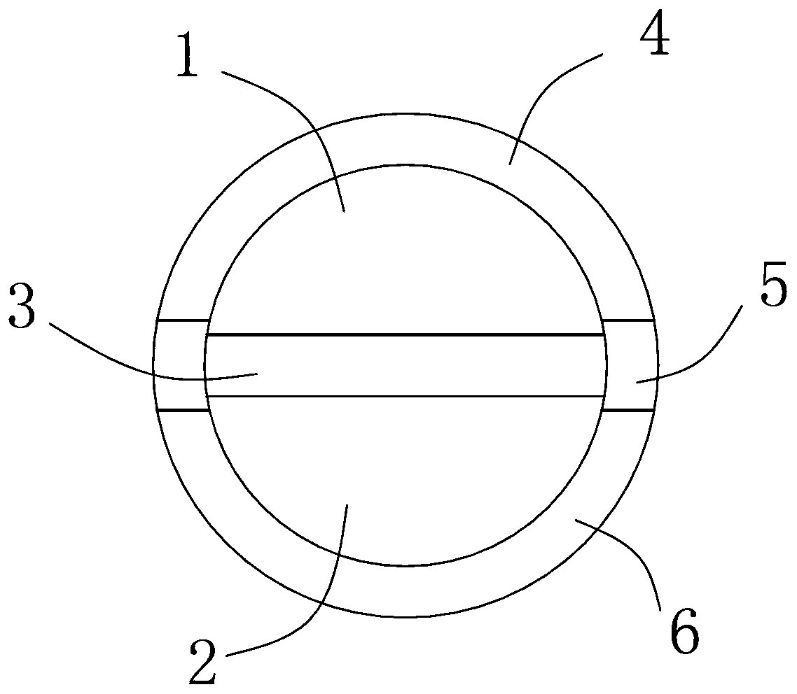
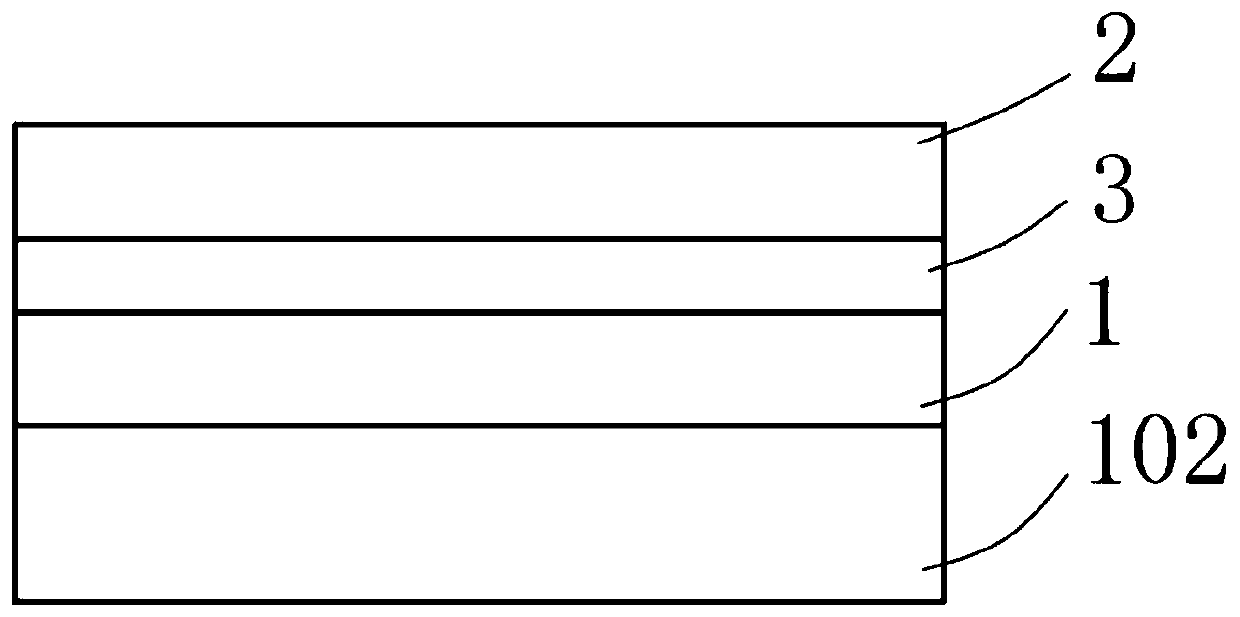
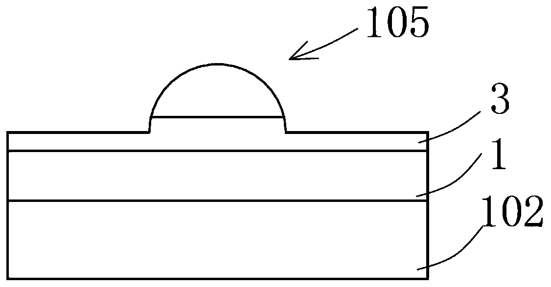
The invention provides a spherical vertical micro LED and a manufacturing method thereof, a display panel and a transfer method thereof. The spherical vertical micro LED comprises a first semiconductor layer, a second semiconductor layer, a light-emitting layer, a first electrode, an insulating layer and a second electrode, the light-emitting layer is arranged between the first semiconductor layerand the second semiconductor layer; the first electrode covers at least part of the surface of the first semiconductor layer, the second electrode covers at least part of the surface of the second semiconductor layer, and the insulating layer covers the light-emitting layer or covers the light-emitting layer and part of the surfaces of the first semiconductor layer and the second semiconductor layer. The first semiconductor layer, the second semiconductor layer and the light-emitting layer form a sphere structure. The first electrode, the insulating layer and the second electrode form a spherical structure covering the outer layer, so that the spherical vertical micro LED is formed, the micro LED is prevented from being clamped outside the loading trap in the transfer process, the micro LED is conveniently and accurately aligned with the loading trap in the transfer process, and the transfer yield and the production efficiency can be effectively improved.

Description

technical field [0001] The present invention relates to the fields of display technology and LED technology, and relates to a spherical vertical micro-LED and a manufacturing method thereof, as well as a display panel including the spherical vertical micro-LED and a transfer method thereof. Background technique [0002] Micro LED, or Micro LED, is an important component of the new generation of display technology. Compared with the existing liquid crystal display, it has better photoelectric efficiency, brightness and contrast, and lower power consumption. It can also be combined with flexible panels to achieve flexible displays. . Therefore, the industry regards Micro LED as the next-generation display technology. [0003] In order to realize the display function, multiple Micro LEDs need to be loaded on the backplane to form a micro LED array. In the process of forming Micro LED arrays, mass transfer technology is the key. At present, mass transfer technologies mainly i...

Claims


Application Information

Patent Timeline
Patent Type & Authority Applications(China)
IPC IPC(8): H01L33/20H01L33/24H01L33/00H01L25/16
CPCH01L25/167H01L33/005H01L33/20H01L33/24H01L25/0753H01L33/007H01L33/0095H01L33/32H01L33/38H01L33/405H01L33/42H01L2933/0016H01L21/67144H01L33/0025H01L33/0075H01L33/40H01L33/44H01L33/0093
Inventor 唐彪许时渊刘海平
Owner CHONGQING KONKA PHOTOELECTRIC TECH RES INST CO LTD
Why Eureka
Try Eureka