
An intelligent correction device control system for super-resolution lithography precision mask

A technology of a calibration device and a control system, which is applied to the exposure device of photoengraving process, the exposure device of microlithography, the components of the TV system, etc., can solve the problems of increasing the workload of the upper computer, reducing the alignment efficiency, and complex implementation steps. , to achieve high-efficiency image acquisition and alignment, improve alignment efficiency, and shorten the control time.

Active Publication Date: 2021-06-18
INST OF OPTICS & ELECTRONICS - CHINESE ACAD OF SCI
View PDF2 Cites 0 Cited by
  • Summary
  • Abstract
  • Description
  • Claims
  • Application Information

AI Technical Summary

Problems solved by technology

The improvement of alignment accuracy and precision overlay accuracy is the main way to improve the exposure efficiency. The technologies to solve the current problems include self-aligned double patterning (SADP) and directional self-assembly (DSA) technology, but the former The implementation steps of the method are complicated, and the required method is costly to implement. The second method is currently incomplete. In this case, it is necessary to improve the alignment accuracy in a faster, low-cost and high-reliability method.
In the current control system, the image processing and acquisition methods mostly use USB serial port transmission or Ethernet port transmission. The transmission speed of these transmission methods is relatively slow, and the efficiency of subsequent processing through the control system will be reduced, and all image processing work is controlled by the host computer. The system is completed, which greatly increases the workload of the upper computer, which will slow down the processing speed of the entire system and reduce the alignment efficiency

Method used


Image

  • An intelligent correction device control system for super-resolution lithography precision mask
  • An intelligent correction device control system for super-resolution lithography precision mask
  • An intelligent correction device control system for super-resolution lithography precision mask

Examples


Embodiment Construction

[0034] The present invention will be described in detail below in conjunction with the accompanying drawings and specific embodiments, but the scope of protection of the present invention is not limited to the following examples, but should include all content in the claims. Moreover, those skilled in the art can realize all the content in the claims from the following embodiment.

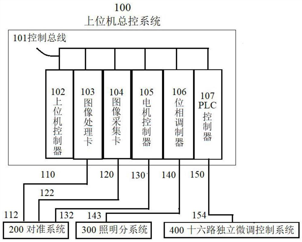
[0035] Such as figure 1 As shown, the precision mask correction device control system of the present invention includes a host computer master control system 100, a control bus 101, a host computer controller 102, an image processing card 103, an image acquisition card 104, a motor controller 105, and a phase modulator 106 , PLC controller 107; the image acquisition card 103 is connected to the outside through the PCIe transmission channel 110, and the image acquisition card 104 is connected to the outside through the Ethernet transmission channel 120; the motor controller 105 is connected to the o...


PUM


Abstract

The invention discloses a control system of an intelligent correction device for a precision mask of super-resolution lithography. The control system combines an optical system to realize accurate control of expected mask deformation. The overall control of the intelligent control system is completed by a high-performance industrial computer. The intelligent control system includes a host computer control system, an image acquisition subsystem, an image processing subsystem, an alignment subsystem, a lighting subsystem and sixteen independent fine-tuning masks. Die deformation control subsystem. Through the combined control of the sub-systems of the control system, the desired precise mask deformation control can be realized, which is simpler and more convenient than the existing realization methods, and the realization of the control system is also more economical. In addition, the control system uses a PCIe channel and an independent graphics card to transmit and process the alignment image signal. The precise deformation control of the mask adopts the PID closed-loop control algorithm to achieve precise regulation, which improves the efficiency of the sub-system and enables the system to be faster and more accurate. Realize mask deformation control and alignment.

Description

technical field [0001] The invention relates to an intelligent control system of a super-resolution lithography machine, in particular to a precision mask correction of the intelligent control system of a lithography machine. Background technique [0002] With the continuous development of the semiconductor industry, lithography machines are the core equipment of semiconductor technology. It can be said that there will be no semiconductors without lithography machines. The lithography machine has experienced the development process of the proximity and contact lithography machine, the stepping and repeating projection lithography machine, and the stepping and scanning lithography machine. The rapid development of lithography machines is also driven by the rapid development of automation and intelligence. With the rapid development of semiconductor integrated circuit technology, higher requirements are put forward for the system design of lithography machines. On the one ha...

Claims


Application Information

Patent Timeline
Patent Type & Authority Patents(China)
IPC IPC(8): G03F9/00G03F7/20H04N5/372
CPCG03F9/7026G03F7/70208H04N25/71G03F7/70783G03F9/7088H04N23/695G05B19/056G05B2219/13004G06T7/0004
Inventor 罗先刚高平蒲明博马晓亮李雄
Owner INST OF OPTICS & ELECTRONICS - CHINESE ACAD OF SCI
Learn More