
Ceramic leadless chip package structure

A packaging structure, leadless technology, used in semiconductor/solid-state device parts, semiconductor devices, electrical components, etc., can solve problems such as performance degradation, achieve high density, reduce packaging process steps, good electrical performance and reliability. Effect

Active Publication Date: 2022-07-08
THE 13TH RES INST OF CHINA ELECTRONICS TECH GRP CORP
View PDF0 Cites 0 Cited by
  • Summary
  • Abstract
  • Description
  • Claims
  • Application Information

AI Technical Summary

Problems solved by technology

[0003] The purpose of the present invention is to provide a ceramic leadless chip package structure, aiming at solving the performance degradation in high-speed and high-frequency applications due to the use of bonding wires for the connection of chips and shell bonding fingers in the prior art technical issues

Method used


Image

  • Ceramic leadless chip package structure
  • Ceramic leadless chip package structure
  • Ceramic leadless chip package structure

Examples


Embodiment Construction

[0041] In order to make the technical problems, technical solutions and beneficial effects to be solved by the present invention clearer, the present invention will be further described in detail below with reference to the accompanying drawings and embodiments. It should be understood that the specific embodiments described herein are only used to explain the present invention, but not to limit the present invention.

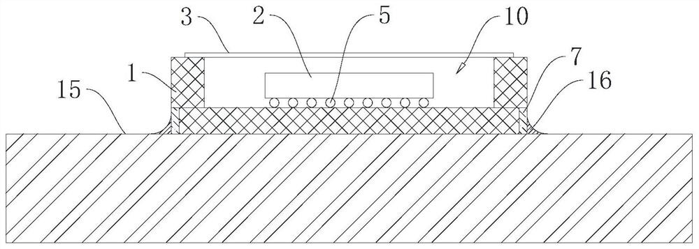
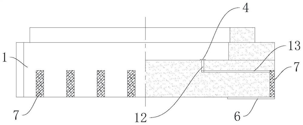
[0042] Please also refer to Figure 1 to Figure 14 , the ceramic leadless chip package structure provided by the present invention will now be described. The ceramic leadless chip package structure includes a ceramic base 1, a chip 2, a lead terminal and a cover plate 3; the ceramic base 1 is provided with a first pad 4, and the back of the chip 2 is provided with a corresponding first pad 4 The second pad is used to weld the first pad 4 through the solder ball 5 after the solder ball 5 is implanted. The first pads 4 are electrically connected, and the cover ...


PUM

PropertyMeasurementUnit
pore sizeaaaaaaaaaa
lengthaaaaaaaaaa

Abstract

The invention provides a ceramic leadless chip packaging structure, belonging to the technical field of chip packaging, comprising a ceramic base, a chip, a lead-out end and a cover plate; the ceramic base is provided with a first pad, and the back of the chip is provided with a first pad The second pad corresponding to the pad, the second pad is used for welding with the first pad through the solder ball after the solder ball is implanted, the lead-out end is arranged at the lower part of the ceramic base, and is connected to the first pad through the conductive structure inside the ceramic base. The pads are conductively connected, and the cover plate is sealed and covered on the periphery of the chip. The ceramic leadless chip packaging structure provided by the present invention avoids the use of bonding wires for bonding, does not cause the problem of performance degradation in high-frequency and high-speed application scenarios caused by bonding wires, reduces packaging process steps, and has more advantages. Good electrical performance and reliability; effectively reduce the size of the ceramic substrate, which is conducive to the miniaturization of the package; because the interconnection form of bonding is changed to the form of flip-chip bump interconnection, the interconnection is greatly improved. density of.

Description

technical field [0001] The invention belongs to the technical field of chip packaging, and more particularly, relates to a ceramic leadless chip packaging structure. Background technique [0002] The ceramic leadless chip case is a miniaturized mounting case. Compared with other package forms, due to its small size, light weight, and outstanding electrical and thermal properties, this package form is suitable for size, weight Therefore, it is very suitable for high-speed, high-performance analog-digital, radio frequency, microwave circuits and other packaging in military and high-reliability fields. The existing ceramic leadless chip package structure chip is arranged in the cavity of the ceramic piece, and the interconnection between the chip and the bonding fingers of the shell is realized through the bonding wire or the silicon aluminum wire, and finally the interconnection between the chip and the external circuit is realized. The existence of the composite wire will br...

Claims


Application Information

Patent Timeline
Patent Type & Authority Patents(China)
IPC IPC(8): H01L23/495H01L23/31H01L23/498
CPCH01L23/49548H01L23/49838H01L23/49816H01L23/3128H01L2224/16225
Inventor 杨振涛
Owner THE 13TH RES INST OF CHINA ELECTRONICS TECH GRP CORP
Learn More