Magnetic memory device
A magnetic storage and magnetic layer technology, applied in the manufacture/processing of electromagnetic devices, resistors controlled by magnetic fields, components of electromagnetic equipment, etc.
- Summary
- Abstract
- Description
- Claims
- Application Information
AI Technical Summary
Problems solved by technology
Method used
Image

Examples
Embodiment Construction
[0013] Embodiments will be described below with reference to the drawings.
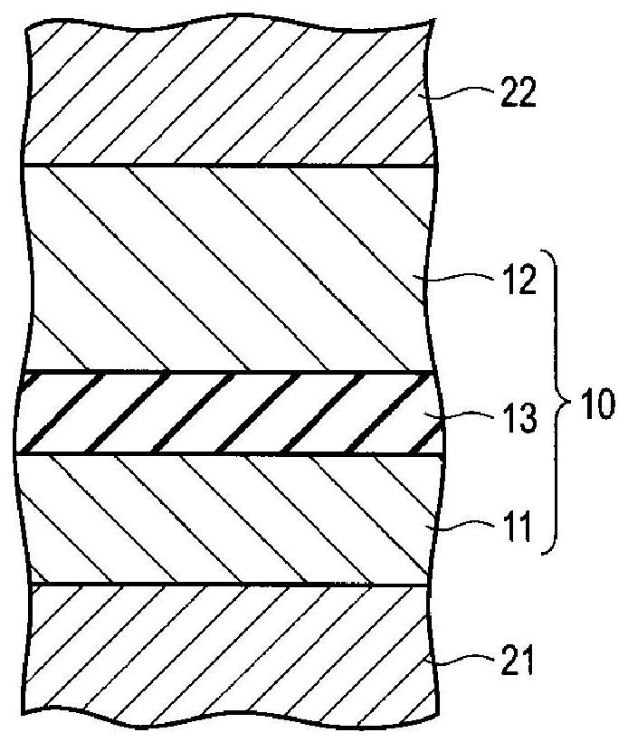
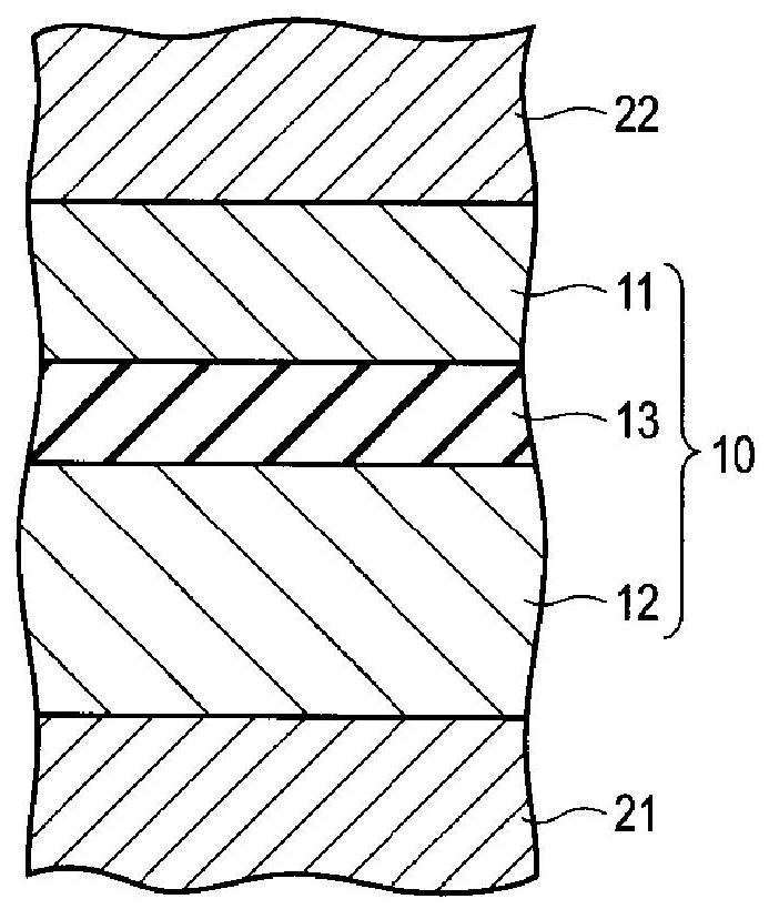
[0014] figure 1 is a cross-sectional view schematically showing the configuration of the magnetic memory device according to the embodiment.
[0015] Such as figure 1 As shown, a laminated structure 10 functioning as a magnetoresistance effect element is provided on an underlying structure (not shown) including a semiconductor substrate, transistors, wiring, and the like. A lower electrode (bottom electrode) 21 and an upper electrode (top electrode) 22 are connected to both ends of the laminated structure 10 . In addition, the magnetoresistance effect element is also called an MTJ (magnetic tunnel junction, magnetic tunnel junction) element. The stacked structure 10 includes a storage layer (first magnetic layer) 11 , a reference layer (second magnetic layer) 12 , and a tunnel barrier layer (nonmagnetic layer) 13 .
[0016] The storage layer (first magnetic layer) 11 has a variable magnetization d...
PUM
 Abstract
Description
Claims
Application Information