Check patentability & draft patents in minutes with Patsnap Eureka AI!

Image sensor pixel structure

An image sensor and pixel structure technology, applied in image communication, electric solid-state devices, semiconductor devices, etc., can solve the problems of CMOS image sensor performance to be improved, and achieve the effect of improving the dynamic range

Active Publication Date: 2020-10-02
BRIGATES MICROELECTRONICS KUNSHAN
View PDF4 Cites 1 Cited by
  • Summary
  • Abstract
  • Description
  • Claims
  • Application Information

AI Technical Summary

Problems solved by technology

[0004] However, the performance of existing CMOS image sensors still needs to be improved

Method used


Image

  • Image sensor pixel structure
  • Image sensor pixel structure
  • Image sensor pixel structure

Examples


Embodiment Construction

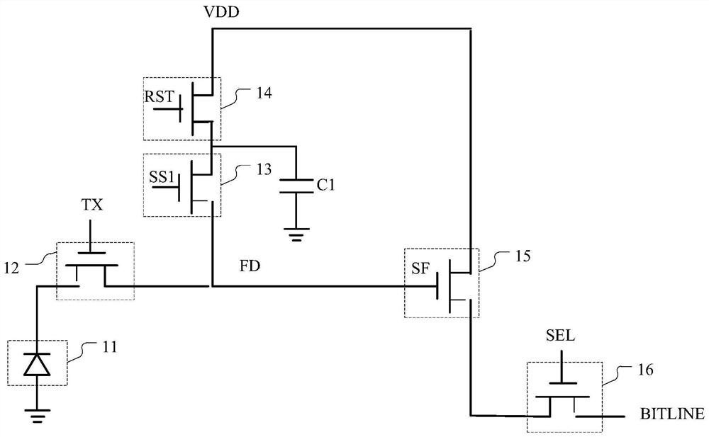
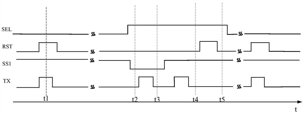
[0044] Dynamic range is a very important index parameter of image sensor. The dynamic range refers to the range of the maximum light intensity and the minimum light intensity that the image sensor can simultaneously detect in the same image, generally expressed in dB. The specific formula is as follows:

[0045]

[0046] Among them, P max Indicates the maximum detectable light intensity, P max Indicates the minimum detectable light intensity. The dynamic range of a general image sensor is between 60-70dB, and the dynamic range of the human eye is between 100-120dB. High dynamic range image sensors are very important for maintaining the balance of details in the dark and details in the bright.

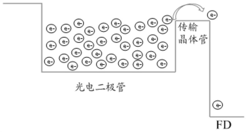
[0047] The full well capacity of an image sensor refers to the maximum number of electrons that can be collected and accommodated by the pixel structure. Large full well capacity can effectively improve the dynamic range of the image sensor. For a general linear response image ...


PUM


Abstract

An image sensor pixel structure is suitable for obtaining N frames of images of the same scene in the same exposure process so as to fuse the obtained N frames of images into one frame of image, and Nis a positive integer and is larger than or equal to 3. The image sensor pixel structure comprises a photoelectric conversion circuit, a transmission circuit, a first charge storage circuit, at leastone second charge storage circuit and a reset circuit, wherein the at least one second charge storage circuit is sequentially connected in series; the first second charge storage circuit is coupled with the first charge storage circuit; and the at least one second charge storage circuit is suitable for respectively storing charges corresponding to the third frame of image to the Nth frame of image in the exposure process. By applying the scheme, the dynamic range of the image sensor can be improved, the signal-to-noise ratio of a dark place of a fused image can be higher, and the image quality is better.

Description

technical field [0001] The invention relates to the field of semiconductor manufacturing, in particular to an image sensor pixel structure. Background technique [0002] An image sensor is a semiconductor device that converts light signals into electrical signals. [0003] Image sensors are classified into complementary metal oxide (Complementary Metal Oxide Semiconductor, CMOS) image sensors and charge coupled device (Charge Coupled Device, CCD) image sensors. Among them, the CMOS image sensor has the advantages of simple process, easy integration of other devices, small size, light weight, low power consumption and low cost. Therefore, with the development of image sensing technology, CMOS image sensors are increasingly used in various electronic products instead of CCD image sensors. At present, CMOS image sensors have been widely used in still digital cameras, digital video cameras, medical imaging devices, and automotive imaging devices. [0004] However, the perform...

Claims


Application Information

Patent Timeline
IPC IPC(8): H04N5/3745H04N5/355H04N5/235H01L27/146
CPCH01L27/14609H01L27/14643H04N23/70H04N25/58H04N25/59H04N25/771
Inventor 黄金德王林胡万景
Owner BRIGATES MICROELECTRONICS KUNSHAN
Features
  • R&D
  • Intellectual Property
  • Life Sciences
  • Materials
  • Tech Scout
  • Unparalleled Data Quality
  • Higher Quality Content
  • 60% Fewer Hallucinations
Learn More