Punching device with positioning and guiding structure

A stamping device and positioning-oriented technology, which is applied in semiconductor/solid-state device manufacturing, electrical components, circuits, etc., can solve the problems of low stamping precision, easy tilting and offset of punches, etc., and achieve the effect of force balance

Inactive Publication Date: 2020-10-13
深圳市尚明精密模具有限公司
View PDF6 Cites 0 Cited by
  • Summary
  • Abstract
  • Description
  • Claims
  • Application Information

AI Technical Summary

Problems solved by technology

[0003] In the existing processing process, the lead frame is moved to the processing position for punching and cutting after being transported by the transfer mechanism, but the existing punch is easy to tilt and shift during the up and down punching process, resulting in low punching accuracy

Method used

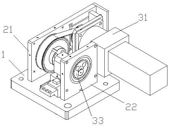
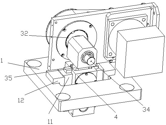
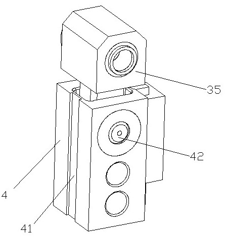

Image

  • Punching device with positioning and guiding structure
  • Punching device with positioning and guiding structure
  • Punching device with positioning and guiding structure

Examples


Embodiment Construction

[0018] In order to make the technical problems, technical solutions and beneficial effects to be solved by the present invention clearer, the present invention will be further described in detail below in conjunction with the accompanying drawings and embodiments. It should be understood that the specific embodiments described here are only used to explain the present invention, not to limit the present invention.

[0019] It should be noted that when an element is referred to as being “fixed” or “disposed on” another element, it may be directly on the other element or be indirectly on the other element. When an element is referred to as being "connected to" another element, it can be directly connected to the other element or indirectly connected to the other element.

[0020] In describing the present invention, it should be understood that the terms "center", "length", "width", "thickness", "upper", "lower", "front", "rear", "left", " The orientation or positional relation...


PUM


Abstract

The invention discloses a punching device with a positioning and guiding structure. The punching device comprises a supporting plate, a driving assembly arranged on the supporting plate and a punchingsleeve head which can be driven by the driving assembly to vertically move back and forth. Sliding grooves are formed in the opposite two sides of the punching sleeve head. Positioning sliding bocksmatched with the sliding grooves are arranged at the positions, corresponding to the opposite two sides of the punching sleeve head, of the supporting plate. By means of the punching device with the positioning and guiding structure, due to the fact that the sliding grooves are formed in the opposite two side faces, in the vertical direction, of the punching sleeve head, and meanwhile the two positioning sliding blocks matched with the sliding grooves are arranged on the supporting plate, the two opposite side faces of the punching sleeve head can be positioned through the positioning slidingblocks, side face supporting force is evenly distributed, it is ensured that deflection cannot happen during vertical motion, and the machining precision and the device stability are effectively improved.

Description

technical field [0001] The invention relates to the field of semiconductor processing, in particular to a stamping device with a positioning and guiding structure. Background technique [0002] Packaging technology is a technology that packages semiconductor integrated circuit chips with insulating plastic or ceramic materials. Packaging technology packaging is necessary and crucial for chips. Because the chip must be isolated from the outside world to prevent impurities in the air from corroding the chip and causing electrical performance degradation. On the other hand, the packaged chip is also easier to install and transport. Lead frame is the most important carrier in packaging technology, and its design structure directly affects the quality and efficiency of packaging technology. [0003] In the existing processing process, the lead frame is moved to the processing position for punching and cutting after being transported by the transfer mechanism, but the existing pu...

Claims


Application Information

Patent Timeline
Patent Type & Authority Applications(China)
IPC IPC(8): B21D28/02B21D28/00H01L21/48
CPCB21D28/002B21D28/02H01L21/4842
Inventor 杨利明
Owner 深圳市尚明精密模具有限公司
Why Eureka
Try Eureka