Three-dimensional memory structure and preparation method thereof

A memory, three-dimensional technology, applied in the direction of electric solid-state devices, semiconductor devices, electrical components, etc., can solve the problems of gate layer breakdown, gate layer short circuit, etc.

Active Publication Date: 2020-10-13
YANGTZE MEMORY TECH CO LTD
View PDF5 Cites 6 Cited by
  • Summary
  • Abstract
  • Description
  • Claims
  • Application Information

AI Technical Summary

Problems solved by technology

[0005] In view of the above-mentioned shortcomings of the prior art, the purpose of the present invention is to provide a three-dimensional memory structure and its preparation method, which is used to solve the problem that the gate layer is easily formed during etching to form contact holes in the existing 3D NAND preparation process. Breakdown, thereby forming a connecting column in the contact hole, will cause a technical problem of shorting between different gate layers

Method used


Image

  • Three-dimensional memory structure and preparation method thereof
  • Three-dimensional memory structure and preparation method thereof
  • Three-dimensional memory structure and preparation method thereof

Examples


Embodiment 1

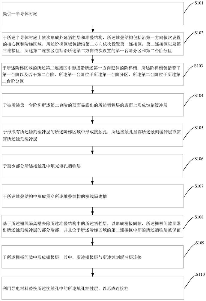
[0156] figure 1 A flow chart of preparing a three-dimensional memory structure according to an embodiment of the present invention is shown. see figure 1 , the preparation method of the three-dimensional memory structure includes:

[0157] Step S101, providing a semiconductor substrate;

[0158] Step S102, sequentially forming an epitaxial sacrificial layer and a stacked structure on the semiconductor substrate, the stacked structure includes alternately stacked interlayer dielectric layers and sacrificial layers, and the stacked structure includes core regions and A stepped area, the stepped area includes a first connection area, a second connection area and a third connection area arranged in sequence along the second direction, and the second connection area includes a first step partition and a second connection area arranged in sequence along the second direction Second step partition;

[0159] Step S103, forming a stepped groove extending along the first direction in...

Embodiment 2

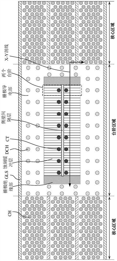
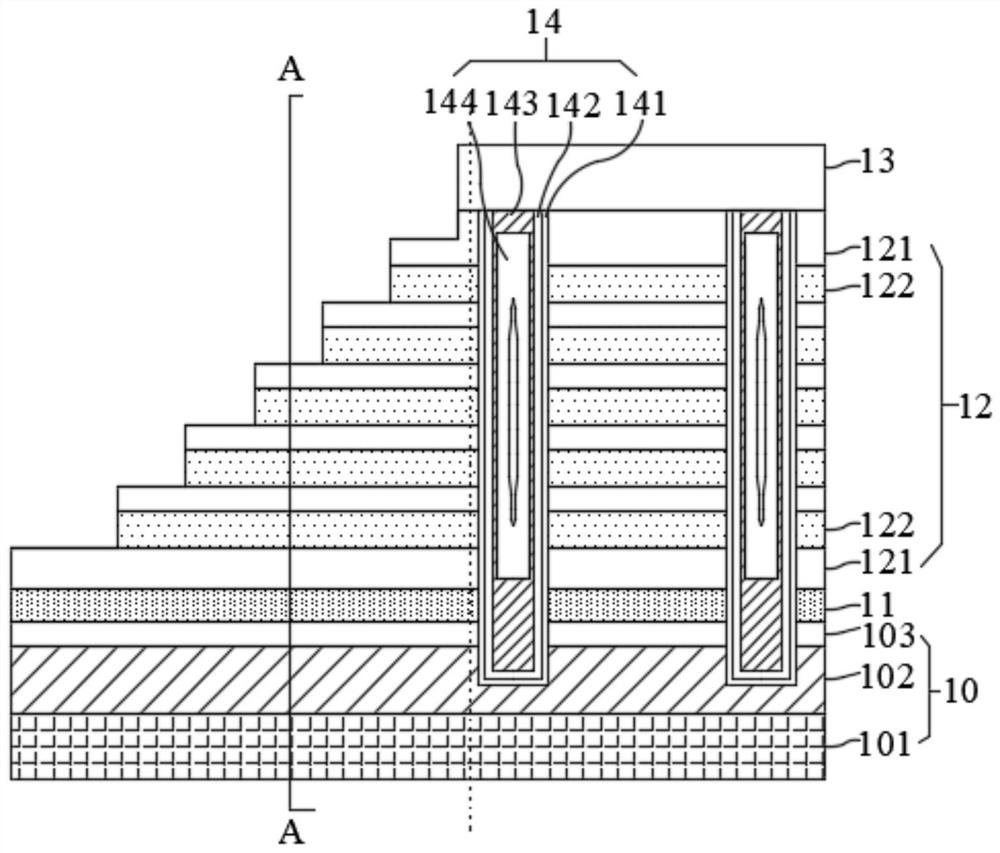
[0198] see figure 2 as well as Figure 31-33 The present invention also provides a three-dimensional memory structure prepared by the preparation method in Embodiment 1. The three-dimensional memory structure at least includes a semiconductor substrate 10, an epitaxial layer 28, a stacked gate structure 30, and several steps (several first steps and several second steps), etch buffer layer 18 and several connection pillars 32 ( figure 2 CT in ). The three-dimensional memory structure of this embodiment can reduce the process difficulty of etching the contact hole 20 in the stepped area, eliminate the word line bridge (Word Line Bridge) of different layers caused when the contact hole 20 is etched during the etching process (Punch), and improve the three-dimensional memory. performance of the piece.

[0199] see figure 2 as well as Figure 31-33 , in this embodiment, the semiconductor substrate 10 includes a substrate body 101, and a doped well is formed in the substrat...


PUM


Abstract

The invention provides a three-dimensional memory structure and a preparation method thereof. The preparation method of a three-dimensional memory structure comprises: dividing the step region into afirst connecting region along a second direction, a second connection area and a third connection area, dividing the second connection area into two step subareas along a second direction, forming anetching buffer layer on the surface of the sacrificial layer of the stacked structure exposed by the top surfaces of the steps of the two step partitions; forming a contact hole in the step region onwhich the etching buffer layer is formed, and when the sacrificial layer of the stacked structure is replaced by the gate conductive material, reserving the sacrificial layer in the middle of the second connection region, and ensuring the gate conductive material to be electrically connected with the etching buffer layer at the edge of the second connection region, so that the connection column inthe contact hole can be electrically connected with the gate layer through the etching buffer layer. By utilizing the method, the process difficulty of etching the contact hole in the step region canbe reduced, and the risk of bridging word lines of different layers during etching of the contact hole is eliminated.

Description

technical field [0001] The invention belongs to the field of semiconductor design and manufacture, and in particular relates to a three-dimensional memory structure and a preparation method thereof. Background technique [0002] In general, a three-dimensional memory includes a gate stack structure formed by alternately stacking gate layers and interlayer dielectric layers, and a contact column (Contact, CT for short) is electrically connected to the gate in a step region of the gate stack structure. However, in the actual manufacturing process of the three-dimensional memory, in order to achieve a good electrical connection between the connecting column and the gate layer in the stacked structure, it is first necessary to etch a contact hole in the dielectric layer covering the stacked gate structure until the contact hole is formed. The hole exposes the surface of the gate layer in the step region, and then the contact hole is filled with a metal material for forming a con...

Claims


Application Information

Patent Timeline
IPC IPC(8): H01L27/11565H01L27/1157H01L27/11582
CPCH10B43/10H10B43/35H10B43/27
Inventor 张坤王迪夏志良周文犀
Owner YANGTZE MEMORY TECH CO LTD
Why Eureka
Try Eureka