Composition for electronic devices, ink for electronic devices, and method for producing electronic device
A technology for electronic devices and compositions, which is applied in the field of compositions for electronic devices, can solve problems such as solvent residues and component performance degradation, and achieve the effects of reduced solvent residues, high liquid stability and component performance
- Summary
- Abstract
- Description
- Claims
- Application Information
AI Technical Summary
Problems solved by technology
Method used
Image

Examples
Embodiment 1
[0489] In Example 1, a thin film was formed from the composition for an electronic device of the present invention, and the remaining amount of the fluorine-containing solvent was evaluated.
[0490]
[0491] A quartz substrate measuring 10 mm in length, 10 mm in width, and 0.7 mm in thickness was ultrasonically cleaned with isopropanol, dried with dry nitrogen, and subjected to UV ozone cleaning for 5 minutes.
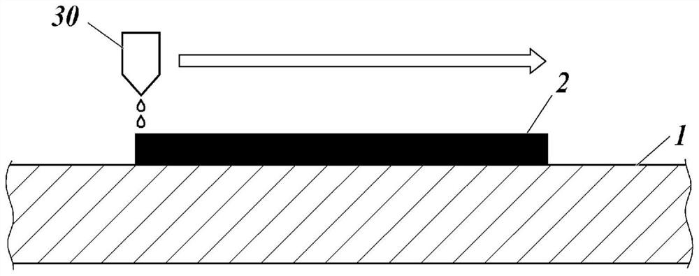
[0492] Compound B1 was dissolved at a concentration of 1% by mass in solvent TFPO as component A according to the present invention under a nitrogen atmosphere. The resulting TFPO solution was used as ink by figure 1 and figure 2 By the inkjet printing method shown in , a film was formed on a quartz substrate so as to have a thickness of 50 nm, and dried at 120° C. for 30 minutes in a nitrogen atmosphere to form a single film 1-1 for evaluation.
[0493]
[0494]In the formation of single membrane 1-1 for evaluation, except that compound B1 was replaced by comp...
Embodiment 2
[0505] In Example 2, the driving of a single-charge device (electronic device only: abbreviated as EOD) incorporating a coating film formed using a composition containing the π-conjugated boron compound and a fluorine-containing solvent according to the present invention voltage, were evaluated.
[0506]
[0507] (formation of anode)
[0508] On a glass substrate with a length of 50 mm, a width of 50 mm, and a thickness of 0.7 mm, ITO (indium tin oxide) was formed into a film with a thickness of 120 nm and patterned to form an anode composed of an ITO transparent electrode. Then, ultrasonic cleaning was performed with isopropanol, dried with dry nitrogen, and UV ozone cleaning was performed for 5 minutes.
[0509] (Formation of hole blocking layer)
[0510] Next, the substrate on which the anode was formed was fixed to a substrate holder of a commercially available vacuum deposition apparatus.
[0511] An optimum amount of calcium was filled in the resistance heating boat...
Embodiment 3
[0525] In Example 3, the stability of the electronic device composition containing the π-conjugated boron compound and the fluorine-containing solvent and the component C according to the present invention was evaluated.
[0526]
[0527] After heating at 85 degreeC in nitrogen atmosphere for 15 minutes, it returned to room temperature, and the following composition 3-1 for evaluation was produced by this.
[0528] (composition 3-1 for evaluation)
[0529] Compound B610 parts by mass
[0530] HFBO2000 parts by mass
[0531]
[0532] In the composition 3-1 for evaluation, except having replaced compound B6 with compound B7, and replaced HFBO with TFPO, the composition 3-2 for evaluation was produced similarly.
[0533] Furthermore, in preparation of evaluation composition 3-2, preparation of evaluation compositions 3-3 to 3-25 was carried out similarly except having replaced compound B7 and TFPO with the compound or solvent described in Table II. In addition, when there ...
PUM
| Property | Measurement | Unit |
|---|---|---|
| thickness | aaaaa | aaaaa |
| thickness | aaaaa | aaaaa |
| thickness | aaaaa | aaaaa |
Abstract
Description
Claims
Application Information